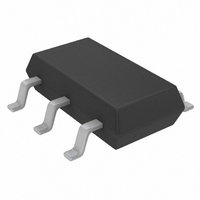
LTC3803ES6#TRMPBF Linear Technology, LTC3803ES6#TRMPBF Datasheet - Page 9

LTC3803ES6#TRMPBF
Manufacturer Part Number
LTC3803ES6#TRMPBF
Description
IC FLYBACK SYNC ADJ 1A TSOT23-6
Manufacturer
Linear Technology
Type
Flybackr
Datasheet
1.LTC3803HS6TRMPBF.pdf
(16 pages)
Specifications of LTC3803ES6#TRMPBF
Internal Switch(s)
No
Synchronous Rectifier
No
Number Of Outputs
1
Voltage - Output
Adjustable
Current - Output
1A
Frequency - Switching
200kHz
Voltage - Input
Adjustable
Operating Temperature
-40°C ~ 85°C
Mounting Type
Surface Mount
Package / Case
TSOT-23-6, TSOT-6
Dc To Dc Converter Type
FLYBACK CONTROLLER
Pin Count
6
Output Current
1A
Package Type
TSOT-23
Mounting
Surface Mount
Operating Temperature Classification
Automotive
Operating Temperature (min)
-40C
Operating Temperature (max)
125C
Lead Free Status / RoHS Status
Lead free / RoHS Compliant
Power - Output
-
Lead Free Status / Rohs Status
Compliant
Other names
LTC3803ES6#PBF
LTC3803ES6#PBF
LTC3803ES6#PBF
Available stocks
Company
Part Number
Manufacturer
Quantity
Price
APPLICATIONS INFORMATION
Many LTC3803 application circuits can be derived from
the topology shown in Figure 2.
The LTC3803 itself imposes no limits on allowed power
output, input voltage V
V
power components. The key factors are: Q1’s maximum
drain-source voltage (BV
and maximum drain current, T1’s saturation fl ux level and
winding insulation breakdown voltages, C
maximum working voltage, ESR, and maximum ripple
current ratings, and D1 and R
SELECTING FEEDBACK RESISTOR DIVIDER VALUES
The regulated output voltage is determined by the resistor
divider across V
of R2 to R1 needed to produce a desired V
calculated:
Choose resistance values for R1 and R2 to be as large as
possible in order to minimize any effi ciency loss due to
the static current drawn from V
so that when V
the nonzero input current to the V
A good rule of thumb is to choose R1 to be 80k or less.
C
OUT
VCC
C
R2 =
C
; these are all determined by the ratings on the external
R3
D2
V
Figure 2. Typical LTC3803 Application Circuit
OUT
1
2
0.8V
R
I
GND
TH
START
R1
– 0.8V
/RUN
LTC3803
OUT
OUT
V
V
V
CC
FB
IN
5
3
NGATE
SENSE
is in regulation, the error caused by
R2
(R1 and R2 in Figure 2). The ratio
IN
• R1
or desired regulated output voltage
6
4
C
DSS
IN
R
L
SL
L
BIAS
PRI
), on-resistance (R
SENSE
OUT
•
•
T1
Q1
R
FB
SENSE
, but just small enough
•
’s power ratings.
L
SEC
pin is less than 1%.
D1
IN
C
OUT
OUT
and C
3803 F02
DS(ON)
can be
OUT
V
OUT
’s
)
TRANSFORMER DESIGN CONSIDERATIONS
Transformer specifi cation and design is perhaps the
most critical part of applying the LTC3803 successfully.
In addition to the usual list of caveats dealing with high
frequency power transformer design, the following should
prove useful.
Turns Ratios
Due to the use of the external feedback resistor divider
ratio to set output voltage, the user has relative freedom
in selecting transformer turns ratio to suit a given appli-
cation. Simple ratios of small integers, e.g., 1:1, 2:1, 3:2,
etc. can be employed which yield more freedom in setting
total turns and mutual inductance. Simple integer turns
ratios also facilitate the use of “off-the-shelf” confi gu-
rable transformers such as the Coiltronics VERSA-PAC™
series in applications with high input to output voltage
ratios. For example, if a 6-winding VERSA-PAC is used
with three windings in series on the primary and three
windings in parallel on the secondary, a 3:1 turns ratio
will be achieved.
Turns ratio can be chosen on the basis of desired duty
cycle. However, remember that the input supply voltage
plus the secondary-to-primary referred version of the
fl yback pulse (including leakage spike) must not exceed
the allowed external MOSFET breakdown rating.
Leakage Inductance
Transformer leakage inductance (on either the primary
or secondary) causes a voltage spike to occur after the
output switch (Q1) turn-off. This is increasingly prominent
at higher load currents, where more stored energy must
be dissipated. In some cases a “snubber” circuit will be
required to avoid overvoltage breakdown at the MOSFET’s
drain node. Application Note 19 is a good reference on
snubber design.
A bifi lar or similar winding technique is a good way to
minimize troublesome leakage inductances. However,
remember that this will limit the primary-to-secondary
breakdown voltage, so bifi lar winding is not always
practical.
LTC3803
3803fc
9


