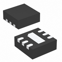
LTC3204BEDC-3.3#TR Linear Technology, LTC3204BEDC-3.3#TR Datasheet - Page 10

LTC3204BEDC-3.3#TR
Manufacturer Part Number
LTC3204BEDC-3.3#TR
Description
IC SW CAP/DBLR 3.3V 50MA 6DFN
Manufacturer
Linear Technology
Type
Switched Capacitor (Charge Pump), Doublerr
Datasheet
1.LTC3204BEDC-5TRMPBF.pdf
(12 pages)
Specifications of LTC3204BEDC-3.3#TR
Internal Switch(s)
Yes
Synchronous Rectifier
No
Number Of Outputs
1
Voltage - Output
3.3V
Current - Output
50mA
Frequency - Switching
1.2MHz
Voltage - Input
1.8 ~ 4.5 V
Operating Temperature
-40°C ~ 85°C
Mounting Type
Surface Mount
Package / Case
6-DFN
Operating Supply Voltage (min)
1.8V
Operating Supply Voltage (max)
4.5V
Operating Temp Range
-40C to 85C
Operating Temperature Classification
Industrial
Pin Count
6
Mounting
Surface Mount
Lead Free Status / RoHS Status
Contains lead / RoHS non-compliant
Power - Output
-
Lead Free Status / Rohs Status
Not Compliant
Available stocks
Company
Part Number
Manufacturer
Quantity
Price
APPLICATIO S I FOR ATIO
LTC3204-3.3/LTC3204-5/
LTC3204B-3.3/LTC3204B-5
Ceramic Capacitors
Ceramic capacitors of different materials lose their capaci-
tance with higher temperature and voltage at different rates.
For example, a capacitor made of X5R or X7R material
will retain most of its capacitance from –40°C to 85°C
whereas a Z5U or Y5V style capacitor will lose considerable
capacitance over that range. Z5U and Y5V capacitors may
also have a poor voltage coefficient causing them to lose
60% or more of their capacitance when the rated voltage
is applied. Therefore when comparing different capacitors,
it is often more appropriate to compare the amount of
achievable capacitance for a given case size rather than
discussing the specified capacitance value. For example,
over rated voltage and temperature conditions, a 1µF 10V
Y5V ceramic capacitor in a 0603 case may not provide any
more capacitance than a 0.22µF 10V X7R capacitor avail-
able in the same 0603 case. In fact, for most LTC3204-3.3/
LTC3204-5/LTC3204B-3.3/LTC3204B-5applications,these
capacitors can be considered roughly equivalent. The
capacitor manufacturer’s data sheet should be consulted
to ensure the desired capacitance at all temperatures and
voltages.
Below is a list of ceramic capacitor manufacturers and
how to contact them:
Layout Considerations
Due to the high switching frequency and high transient
currentsproducedbyLTC3204-3.3/LTC3204-5/LTC3204B-
3.3/LTC3204B-5, careful board layout is necessary for
optimum performance. A true ground plane and short
connections to all the external capacitors will improve per-
formanceandensureproperregulationunderallconditions.
Figure 4 shows an example layout for the LTC3204-3.3/
LTC3204-5/LTC3204B-3.3/LTC3204B-5.
10
AVX
Kemet
Murata
Taiyo Yuden
Vishay
TDK
U
U
www.avxcorp.com
www.kemet.com
www.murata.com
www.t-yuden.com
www.vishay.com
www.component.tdk.com
W
U
Thermal Management
For higher input voltages and maximum output cur-
rent, there can be substantial power dissipation in the
LTC3204-3.3/LTC3204-5/LTC3204B-3.3/LTC3204B-5. If
the junction temperature increases above approximately
160°C, the thermal shutdown circuitry will automatically
deactivate the output. To reduce the maximum junction
temperature, a good thermal connection to the PC board
is recommended. Connecting the GND pin (Pin 1) and
the exposed pad of the DFN package (Pin 7) to a ground
plane under the device on two layers of the PC board
can reduce the thermal resistance of the package and PC
board considerably.
Derating Power at High Temperatures
To prevent an overtemperature condition in high power
applications, Figure 5 should be used to determine the
maximum combination of ambient temperature and power
dissipation.
The power dissipated in the LTC3204-3.3/LTC3204-5/
LTC3204B-3.3/LTC3204B-5 should always fall under the
line shown for a given ambient temperature. The power
dissipation in the LTC3204-3.3/ LTC3204-5/LTC3204B-3.3/
LTC3204B-5 is given by the expression:
This derating curve assumes a maximum thermal resis-
tance, θ
P
D
V
= (
OUT
V
IN
JA
2
, of 80°C/W for the 2mm × 2mm DFN package.
V
IN
0603
C
0603
–
C
Figure 4. Recommended Layout
OUT
IN
V
OUT
GND
)•
I
OUT
C
+
C
–
3204 F04
C
0603
FLY
SHDN
3204fa


