LTC3204BEDC-3.3#TR Linear Technology, LTC3204BEDC-3.3#TR Datasheet - Page 11
LTC3204BEDC-3.3#TR
Manufacturer Part Number
LTC3204BEDC-3.3#TR
Description
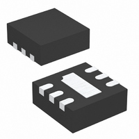
IC SW CAP/DBLR 3.3V 50MA 6DFN
Manufacturer
Linear Technology
Type
Switched Capacitor (Charge Pump), Doublerr
Datasheet
1.LTC3204BEDC-5TRMPBF.pdf
(12 pages)
Specifications of LTC3204BEDC-3.3#TR
Internal Switch(s)
Yes
Synchronous Rectifier
No
Number Of Outputs
1
Voltage - Output
3.3V
Current - Output
50mA
Frequency - Switching
1.2MHz
Voltage - Input
1.8 ~ 4.5 V
Operating Temperature
-40°C ~ 85°C
Mounting Type
Surface Mount
Package / Case
6-DFN
Operating Supply Voltage (min)
1.8V
Operating Supply Voltage (max)
4.5V
Operating Temp Range
-40C to 85C
Operating Temperature Classification
Industrial
Pin Count
6
Mounting
Surface Mount
Lead Free Status / RoHS Status
Contains lead / RoHS non-compliant
Power - Output
-
Lead Free Status / Rohs Status
Not Compliant
Available stocks
Company
Part Number
Manufacturer
Quantity
Price


APPLICATIO S I FOR ATIO
This can be achieved from a printed circuit board layout
with a solid ground plane and a good connection to the
ground pins of LTC3204-3.3/LTC3204-5/LTC3204B-3.3/
LTC3204B-5 and the exposed pad of the DFN package.
PACKAGE DESCRIPTIO
2.50 ±0.05
1.15 ±0.05
RECOMMENDED SOLDER PAD PITCH AND DIMENSIONS
NOTE:
1. DRAWING TO BE MADE A JEDEC PACKAGE OUTLINE M0-229 VARIATION OF (WCCD-2)
2. DRAWING NOT TO SCALE
3. ALL DIMENSIONS ARE IN MILLIMETERS
4. DIMENSIONS OF EXPOSED PAD ON BOTTOM OF PACKAGE DO NOT INCLUDE
5. EXPOSED PAD SHALL BE SOLDER PLATED
6. SHADED AREA IS ONLY A REFERENCE FOR PIN 1 LOCATION ON THE
MOLD FLASH. MOLD FLASH, IF PRESENT, SHALL NOT EXCEED 0.15mm ON ANY SIDE
TOP AND BOTTOM OF PACKAGE
0.61 ±0.05
(2 SIDES)
U
U
1.42 ±0.05
(2 SIDES)
Information furnished by Linear Technology Corporation is believed to be accurate and reliable. However,
no responsibility is assumed for its use. Linear Technology Corporation makes no representation that
the interconnection of its circuits as described herein will not infringe on existing patent rights.
0.50 BSC
W
0.25 ± 0.05
0.675 ±0.05
U
PACKAGE
OUTLINE
Figure 5. Maximum Power Dissipation
3.0
2.5
2.0
1.5
1.0
0.5
0
6-Lead Plastic DFN (2mm × 2mm)
–50
(Reference LTC DWG # 05-08-1703)
U
(SEE NOTE 6)
TOP MARK
vs Ambient Temperature
PIN 1 BAR
–25
AMBIENT TEMPERATURE (C)
0.200 REF
0
DC Package
25
50
Operation out of this curve will cause the junction tem-
perature to exceed 160°C which may trigger the thermal
shutdown.
75
LTC3204B-3.3/LTC3204B-5
100 125 150
LTC3204-3.3/LTC3204-5/
0.75 ±0.05
3204 G05
2.00 ±0.10
(4 SIDES)
0.00 – 0.05
0.56 ± 0.05
(2 SIDES)
R = 0.115
BOTTOM VIEW—EXPOSED PAD
TYP
1.37 ±0.05
(2 SIDES)
3
4
6
1
0.50 BSC
0.38 ± 0.05
0.25 ± 0.05
PIN 1
CHAMFER OF
EXPOSED PAD
11
(DC6) DFN 1103
3204fa
Related parts for LTC3204BEDC-3.3#TR
Image
Part Number
Description
Manufacturer
Datasheet
Request
R

Part Number:
Description:
IC SW CAP/DBLR 5V .15A 6DFN
Manufacturer:
Linear Technology
Datasheet:
Part Number:
Description:
IC SW CAP/DBLR 3.3V 50MA 6DFN
Manufacturer:
Linear Technology
Datasheet:
Part Number:
Description:
IC SW CAP/DBLR 3.3V 50MA 6DFN
Manufacturer:
Linear Technology
Datasheet:
Part Number:
Description:
IC SW CAP/DBLR 5V .15A 6DFN
Manufacturer:
Linear Technology
Datasheet:
Part Number:
Description:
IC SW CAP/DBLR 3.3V 50MA 6DFN
Manufacturer:
Linear Technology
Datasheet:
Part Number:
Description:
IC SW CAP/DBLR 5V .15A 6DFN
Manufacturer:
Linear Technology
Datasheet:
Part Number:
Description:
IC SW CAP/DBLR 5V .15A 6DFN
Manufacturer:
Linear Technology
Datasheet:

Part Number:
Description:
Manufacturer:
Linear Technology
Datasheet:
Part Number:
Description:
Manufacturer:
Linear Technology
Datasheet:

Part Number:
Description:
Low Noise Regulated Charge Pump In 2 ? 2 Dfn
Manufacturer:
Linear Technology Corporation
Datasheet:
Part Number:
Description:
CD ROM LINEARVIEW DATASHEETS
Manufacturer:
Linear Technology
Part Number:
Description:
Standalone Linear Li-Ion Battery Charger with Thermal Regulation in ThinSOT
Manufacturer:
Linear Technology Corporation
Datasheet:
Part Number:
Description:
Low noise, high frequency, 8th order linear phase lowpass filter
Manufacturer:
Linear Technology Corporation
Datasheet:
Part Number:
Description:
Manufacturer:
Linear Technology Corporation
Datasheet:
Part Number:
Description:
Manufacturer:
Linear Technology Corporation
Datasheet: