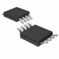
LT1317BCMS8 Linear Technology, LT1317BCMS8 Datasheet - Page 10

LT1317BCMS8
Manufacturer Part Number
LT1317BCMS8
Description
IC BOOST ADJ .5A 8MSOP
Manufacturer
Linear Technology
Type
Step-Up (Boost)r
Datasheet
1.LT1317CS8PBF.pdf
(16 pages)
Specifications of LT1317BCMS8
Internal Switch(s)
Yes
Synchronous Rectifier
No
Number Of Outputs
1
Voltage - Output
1.24 ~ 30 V
Current - Output
500mA
Frequency - Switching
620kHz
Voltage - Input
1.5 ~ 12 V
Operating Temperature
0°C ~ 70°C
Mounting Type
Surface Mount
Package / Case
8-MSOP, Micro8™, 8-uMAX, 8-uSOP,
Lead Free Status / RoHS Status
Contains lead / RoHS non-compliant
Power - Output
-
Available stocks
Company
Part Number
Manufacturer
Quantity
Price
Company:
Part Number:
LT1317BCMS8
Manufacturer:
LT
Quantity:
5 321
Company:
Part Number:
LT1317BCMS8
Manufacturer:
LT
Quantity:
10 000
Part Number:
LT1317BCMS8
Manufacturer:
LINEAR/凌特
Quantity:
20 000
Company:
Part Number:
LT1317BCMS8 (LTHB)
Manufacturer:
a
Quantity:
4
Company:
Part Number:
LT1317BCMS8#PBF
Manufacturer:
LT
Quantity:
3
Part Number:
LT1317BCMS8#PBF
Manufacturer:
LINEAR/凌特
Quantity:
20 000
Company:
Part Number:
LT1317BCMS8#TRPBF
Manufacturer:
TI
Quantity:
2 999
Part Number:
LT1317BCMS8#TRPBF
Manufacturer:
LT凌特厂
Quantity:
20 000
APPLICATIONS
LT1317/LT1317B
FREQUENCY COMPENSATION
The LT1317 has an external compensation pin (V
allows the frequency response to be optimized for the
circuit configuration. In most cases, the values used in
Figure 1 will work. Some circuits may need additional
compensation and a simple trial and error method for
determining the necessary component values is given.
Figure 6 shows the test setup. A load step is applied and
the resulting output voltage waveform is observed. Fig-
ures 7 through 10 detail the response for various values of
R and C in the compensation network. The circuit of
Figure 7 starts with a large C and small R giving a highly
overdamped system. This system will always be stable but
the output voltage displays a long settling time of >5ms.
Figure 8’s circuit has reduced C giving a shorter settling
time but still overdamped. Figure 9 shows the results
when C is reduced to the point where the system becomes
underdamped. The output voltage responds quickly
( 200 s to 300 s) but some ringing exists. Figure 10 has
AC COUPLED
AC COUPLED
10
100mV/DIV
100mV/DIV
2mA TO
2mA TO
200mA
200mA
I
I
V
V
LOAD
LOAD
OUT
OUT
Figure 9. Using 680pF for C Results in an
Underdamped System with Ringing. (R = 33k)
Figure 7. With C = 56nF and R = 33k,
the System is Highly Overdamped.
U
INFORMATION
U
5ms/DIV
1ms/DIV
W
1317 F07
1317 F09
U
C
) which
optimum R and C values giving the best possible settling
time with adequate phase margin.
An additional 100pF capacitor (C
pin and is necessary if the LT1317 is operated near current
limit. Also, C
capacitors are used.
AC COUPLED
AC COUPLED
100mV/DIV
100mV/DIV
V
2V
IN
2mA TO
2mA TO
200mA
200mA
+
I
I
V
V
LOAD
LOAD
OUT
OUT
47 F
Figure 6. Frequency Response Test Setup
Figure 10. 3.3nF and 33k Gives the
Shortest Settling Time with No Ringing.
C
100pF
C2
C2
Figure 8. Reducing C to 22nF
Speeds Up the Response. (R = 33k)
should be present when higher ESR output
SHDN
V
V
IN
C
R
LT1317
C
10 H
GND
SW
MBR0520L
FB
5ms/DIV
1ms/DIV
C2
1M
604k
) is connected to the V
+
47 F
15
2W
1317 F08
1317 F10
V
3.3V
OUT
50
1317 F06
C


