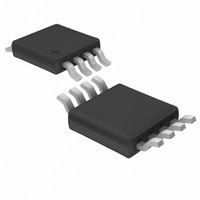
LT1317BCMS8 Linear Technology, LT1317BCMS8 Datasheet - Page 8

LT1317BCMS8
Manufacturer Part Number
LT1317BCMS8
Description
IC BOOST ADJ .5A 8MSOP
Manufacturer
Linear Technology
Type
Step-Up (Boost)r
Datasheet
1.LT1317CS8PBF.pdf
(16 pages)
Specifications of LT1317BCMS8
Internal Switch(s)
Yes
Synchronous Rectifier
No
Number Of Outputs
1
Voltage - Output
1.24 ~ 30 V
Current - Output
500mA
Frequency - Switching
620kHz
Voltage - Input
1.5 ~ 12 V
Operating Temperature
0°C ~ 70°C
Mounting Type
Surface Mount
Package / Case
8-MSOP, Micro8™, 8-uMAX, 8-uSOP,
Lead Free Status / RoHS Status
Contains lead / RoHS non-compliant
Power - Output
-
Available stocks
Company
Part Number
Manufacturer
Quantity
Price
Company:
Part Number:
LT1317BCMS8
Manufacturer:
LT
Quantity:
5 321
Company:
Part Number:
LT1317BCMS8
Manufacturer:
LT
Quantity:
10 000
Part Number:
LT1317BCMS8
Manufacturer:
LINEAR/凌特
Quantity:
20 000
Company:
Part Number:
LT1317BCMS8 (LTHB)
Manufacturer:
a
Quantity:
4
Company:
Part Number:
LT1317BCMS8#PBF
Manufacturer:
LT
Quantity:
3
Part Number:
LT1317BCMS8#PBF
Manufacturer:
LINEAR/凌特
Quantity:
20 000
Company:
Part Number:
LT1317BCMS8#TRPBF
Manufacturer:
TI
Quantity:
2 999
Part Number:
LT1317BCMS8#TRPBF
Manufacturer:
LT凌特厂
Quantity:
20 000
APPLICATIONS
LT1317/LT1317B
The LT1317B differs from the LT1317 in that the bias point
on A1 is set lower than on the LT1317 so that minimum
switch current can drop below 50mA. Because A1’s bias
point is set lower, there is no Burst Mode operation at light
loads and the device continues switching at constant
frequency. This results in the absence of low frequency
output voltage ripple at the expense of light load efficiency.
The difference between the two devices is clearly illus-
trated in Figure 2. The top two traces in Figure 2 show an
LT1317/LT1317B circuit, using the components indicated
in Figure 1, set to a 3.3V output. Input voltage is 2V. Load
current is stepped from 2mA to 200mA for both circuits.
Low frequency Burst Mode operation voltage ripple is
observed on Trace A, while none is observed on Trace B.
LAYOUT HINTS
The LT1317 switches current at high speed, mandating
careful attention to layout for proper performance. You
will not get advertised performance with careless layouts.
Figure 3 shows recommended component placement.
Follow this closely in your PC layout. Note the direct path
of the switching loops. Input capacitor C
close (< 5mm) to the IC package. As little as 10mm of wire
or PC trace from C
inability to regulate or oscillation.
8
TRACE B
TRACE A
I
LOAD
Figure 2. LT1317 Exhibits Ripple at 2mA Load
During Burst Mode Operation, the LT1317B Does Not
AC COUPLED
AC COUPLED
100mV/DIV
100mV/DIV
LT1317B
LT1317
200mA
V
V
2mA
OUT
OUT
IN
U
to V
INFORMATION
IN
U
will cause problems such as
1ms/DIV
W
IN
must be placed
U
1317 F02
Figure 3. Recommended Component Placement. Traces Carrying
High Current Are Direct. Trace Area at FB Pin and V
Low. Lead Length to Battery Should be Kept Short.
COMPONENT SELECTION
Inductors
Inductors appropriate for use with the LT1317 must
possess three attributes. First, they must have low core
loss at 600kHz. Most ferrite core units have acceptable
losses at this switching frequency. Inexpensive iron pow-
der cores should be viewed suspiciously, as core losses
can cause significant efficiency penalties at 600kHz. Sec-
ond, the inductor must be able to handle peak switch
current of the LT1317 without saturating. This places a
lower limit on the physical size of the unit. Molded chokes
or chip inductors usually do not have enough core to
support the LT1317 maximum peak switch current and are
unsuitable for the application. Lastly, the inductor should
have low DCR (copper wire resistance) to prevent effi-
ciency-killing I
several inductors suitable for use with the LT1317. This is
not an exclusive list. There are many magnetics vendors
whose components are suitable for use. A few vendor’s
components are listed in Table 1.
MULTIPLE
VIAs
2
R losses. Linear Technology has identified
1
2
3
4
GND
GROUND PLANE
C
IN
LT1317
C
OUT
8
7
6
5
V
L
OUT
D
C
Pin is Kept
1317 F03
V
IN


