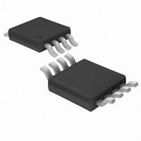
LT1317BCMS8 Linear Technology, LT1317BCMS8 Datasheet - Page 7

LT1317BCMS8
Manufacturer Part Number
LT1317BCMS8
Description
IC BOOST ADJ .5A 8MSOP
Manufacturer
Linear Technology
Type
Step-Up (Boost)r
Datasheet
1.LT1317CS8PBF.pdf
(16 pages)
Specifications of LT1317BCMS8
Internal Switch(s)
Yes
Synchronous Rectifier
No
Number Of Outputs
1
Voltage - Output
1.24 ~ 30 V
Current - Output
500mA
Frequency - Switching
620kHz
Voltage - Input
1.5 ~ 12 V
Operating Temperature
0°C ~ 70°C
Mounting Type
Surface Mount
Package / Case
8-MSOP, Micro8™, 8-uMAX, 8-uSOP,
Lead Free Status / RoHS Status
Contains lead / RoHS non-compliant
Power - Output
-
Available stocks
Company
Part Number
Manufacturer
Quantity
Price
Company:
Part Number:
LT1317BCMS8
Manufacturer:
LT
Quantity:
5 321
Company:
Part Number:
LT1317BCMS8
Manufacturer:
LT
Quantity:
10 000
Part Number:
LT1317BCMS8
Manufacturer:
LINEAR/凌特
Quantity:
20 000
Company:
Part Number:
LT1317BCMS8 (LTHB)
Manufacturer:
a
Quantity:
4
Company:
Part Number:
LT1317BCMS8#PBF
Manufacturer:
LT
Quantity:
3
Part Number:
LT1317BCMS8#PBF
Manufacturer:
LINEAR/凌特
Quantity:
20 000
Company:
Part Number:
LT1317BCMS8#TRPBF
Manufacturer:
TI
Quantity:
2 999
Part Number:
LT1317BCMS8#TRPBF
Manufacturer:
LT凌特厂
Quantity:
20 000
APPLICATIONS
BLOCK
OPERATION
The LT1317 combines a current mode, fixed frequency
PWM architecture with Burst Mode micropower operation
to maintain high efficiency at light loads. Operation can
best be understood by referring to the Block Diagram.
The error amplifier compares voltage at the FB pin with the
internal 1.24V bandgap reference and generates an error
signal V
hysteretic comparator A1, A1’s output goes low, turning
off all circuitry except the 1.24V reference, error amplifier
and low-battery detector. Total current consumption in
this state is 100 A. As output loading causes the FB
voltage to decrease, V
go high, in turn enabling the rest of the IC. Switch current
is limited to approximately 250mA initially after A1’s
output goes high. If the load is light, the output voltage
(and FB voltage) will increase until A1’s output goes low,
turning off the rest of the LT1317. Low frequency ripple
voltage appears at the output. The ripple frequency is
dependent on load current and output capacitance. This
Burst Mode operation keeps the output regulated and
reduces average current into the IC, resulting in high
efficiency even at load currents of 300 A or less.
C
. When V
DIAGRAM
V
OUT
REFERENCE
R1
(EXTERNAL)
R2
(EXTERNAL)
1.24V
C
U
FB
decreases below the bias voltage on
C
increases causing A1’s output to
INFORMATION
U
W
FB
2
–
+
OSCILLATOR
GENERATOR
W
600kHz
RAMP
g
AMPLIFIER
m
ERROR
U
+
+
BIAS
V
+
–
–
+
1
C
If the output load increases sufficiently, A1’s output remains
high, resulting in continuous operation. When the LT1317
is running continuously, peak switch current is controlled
by V
on at the beginning of each switch cycle. When the sum-
mation of a signal representing switch current and a ramp
generator (introduced to avoid subharmonic oscillations at
duty factors greater than 50%) exceeds the V
comparator A2 changes state, resetting the flip-flop and
turning off the switch. Output voltage increases as switch
current is increased. The output, attenuated by a resistor
divider, appears at the FB pin, closing the overall loop.
Frequency compensation is provided by an external series
RC network and an optional capacitor connected between
the V
Low-battery detector A4’s open collector output (LBO) pulls
low when the LBI pin voltage drops below 200mV. There
is no hysteresis in A4, allowing it to be used as an amplifier
in some applications. The low-battery detector remains
active in shutdown. To enable the converter, SHDN must
be left floating or tied to a voltage between 1.4V and 6V.
A2
COMPARATOR
A1
COMPARATOR
C
C
to regulate the output voltage. The switch is turned
pin and ground.
ENABLE
200mV
R
FF
S
LBI
7
Q
–
+
A = 2
SHUTDOWN
A4
+
–
LT1317/LT1317B
DRIVER
SHDN
GND
LBO
SW
8
3
5
4
Q3
0.08
1317 BD
C
signal,
7


