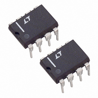
LTC1147CN8-5 Linear Technology, LTC1147CN8-5 Datasheet

LTC1147CN8-5
Specifications of LTC1147CN8-5
Related parts for LTC1147CN8-5
LTC1147CN8-5 Summary of contents
Page 1
... V = 10V ( operation are typically 0mA to 300mA. For applications where even higher efficiency is required, refer to the LTC1148 data sheet and Application Note 54. , LTC and LT are registered trademarks of Linear Technology Corporation. Burst Mode is a trademark of Linear Technology Corporation. *LTC1147L and LTC1147L-3.3 only 100 F ...
Page 2
... U Operating Ambient Temperature Range LTC1147C ............................................... LTC1147I ............................................. – Extended Commercial + 0.3V) to – 0.3V Temperature Range (Note 4) ................. – Junction Temperature (Note 1) ............................ 125 C Storage Temperature Range ................ – 150 C Lead Temperature (Soldering, 10 sec)................. 300 ORDER PART NUMBER LTC1147CN8-3.3 LTC1147CN8-5 LTC1147CS8-3.3 + LTC1147CS8-5 LTC1147IS8-3 10V CONDITIONS ...
Page 3
... OFF The denotes specifications which apply over the full specified temperature range. Note calculated from the ambient temperature T J dissipation P according to the following formulas: D LTC1147CN8-3.3/LTC1147CN8- LTC1147LIS/LTC1147IS8/LTC1147LCS/ LTC1147CS8-3.3/LTC1147CS8- Note 2: Dynamic supply current is higher due to the gate charge being delivered at the switching frequency. See Applications Information. ...
Page 4
LTC1147-3.3 LTC1147-5/LTC1147L W U TYPICAL PERFOR A CE CHARACTERISTICS Efficiency vs Input Voltage 100 FIGURE 1 CIRCUIT LOAD 100mA LOAD ...
Page 5
CTIO S V (Pin 1): Main Supply Pin. Must be closely decoupled IN to ground Pin 7. C (Pin 2): External capacitor C from Pin 2 to ground sets T T the operating frequency. The ...
Page 6
LTC1147-3.3 LTC1147-5/LTC1147L U OPERATIO (Refer to Functional Diagram) The LTC1147 series uses a current mode, constant off- time architecture to switch an external P-channel power MOSFET. Operating frequency is set by an external capaci- tor at C (Pin 2). T ...
Page 7
U U APPLICATIO S I FOR ATIO The basic LTC1147 application circuit is shown in Figure 1. External component selection is driven by the load requirement and begins with the selection known, C and L can ...
Page 8
LTC1147-3.3 LTC1147-5/LTC1147L U U APPLICATIO S I FOR ATIO 1000 V SENSE – 800 600 400 V = 12V IN 200 200 100 FREQUENCY (kHz) Figure 3. Timing Capacitor Value is given by: V ...
Page 9
U U APPLICATIO S I FOR ATIO used. For V > 8V, a standard threshold MOSFET (V IN < 4V) may be used expected to drop below 8V logic-level threshold MOSFET (V strongly recommended. When ...
Page 10
LTC1147-3.3 LTC1147-5/LTC1147L U U APPLICATIO S I FOR ATIO Optimum efficiency is obtained by making the ESR equal the ESR is increased SENSE efficiency degrades by less than 1%. If the ESR is ...
Page 11
U U APPLICATIO S I FOR ATIO where L1, L2, etc., are the individual losses as a percent- age of input power. (For high efficiency circuits only small errors are incurred by expressing losses as a percentage of output power.) ...
Page 12
LTC1147-3.3 LTC1147-5/LTC1147L U U APPLICATIO S I FOR ATIO Other losses including C and C IN losses, MOSFET switching losses, and inductor core losses, generally account for less than 2% total additional loss. Design Example As a design example, assume ...
Page 13
U U APPLICATIO S I FOR ATIO Board Layout Checklist When laying out the printed circuit board, the following checklist should be used to ensure proper operation of the LTC1147 series. These items are also illustrated graphi- cally in the ...
Page 14
LTC1147-3.3 LTC1147-5/LTC1147L U TYPICAL APPLICATIO 120pF 3300pF SUMIDA CDR74B-100LC ** IRC LRC-LR2010-01-R068-F Precision Constant Current Source 0.1 F LTC1147L 1 PDRIVE GND C T ...
Page 15
... MOLD FLASH OR PROTRUSIONS SHALL NOT EXCEED 0.010 INCH (0.254mm) Information furnished by Linear Technology Corporation is believed to be accurate and reliable. However, no responsibility is assumed for its use. Linear Technology Corporation makes no represen- tation that the interconnection of its circuits as described herein will not infringe on existing patent rights. ...
Page 16
... Standard Threshold FETs IN Synchronous, V 40V for Logic Level MOSFETS IN 0.5A Switch, V 18.5V, Comparator IN 1.2A Switch, V 13V, Comparator IN Dual Version of LTC1159 16-Pin Narrow SO/SSOP; Constant Frequency sn1147 1147fds LT/TP 0698 REV D 2K • PRINTED IN USA LINEAR TECHNOLOGY CORPORATION 1993 SO8 0996 ...


