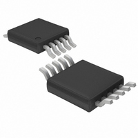
LTC3411EMS#TRPBF Linear Technology, LTC3411EMS#TRPBF Datasheet - Page 15

LTC3411EMS#TRPBF
Manufacturer Part Number
LTC3411EMS#TRPBF
Description
IC CONV DC/DC SYNC STPDWN 10MSOP
Manufacturer
Linear Technology
Type
Step-Down (Buck)r
Datasheet
1.LTC3411EDDPBF.pdf
(24 pages)
Specifications of LTC3411EMS#TRPBF
Internal Switch(s)
Yes
Synchronous Rectifier
Yes
Number Of Outputs
1
Voltage - Output
0.8 ~ 5 V
Current - Output
1.25A
Frequency - Switching
1MHz
Voltage - Input
2.63 ~ 5.5 V
Operating Temperature
-40°C ~ 85°C
Mounting Type
Surface Mount
Package / Case
10-MSOP, Micro10™, 10-uMAX, 10-uSOP
Lead Free Status / RoHS Status
Lead free / RoHS Compliant
Power - Output
-
Available stocks
Company
Part Number
Manufacturer
Quantity
Price
APPLICATIONS INFORMATION
In some applications, a more severe transient can be caused
by switching in loads with large (>1uF) input capacitors.
The discharged input capacitors are effectively put in paral-
lel with C
can deliver enough current to prevent this problem, if the
switch connecting the load has low resistance and is driven
quickly. The solution is to limit the turn-on speed of the load
switch driver. A hot swap controller is designed specifi cally
for this purpose and usually incorporates current limiting,
short-circuit protection, and soft-starting.
Effi ciency Considerations
The percent effi ciency of a switching regulator is equal to
the output power divided by the input power times 100%.
It is often useful to analyze individual losses to determine
what is limiting the effi ciency and which change would
produce the most improvement. Percent effi ciency can
be expressed as:
where L1, L2, etc. are the individual losses as a percent-
age of input power.
Although all dissipative elements in the circuit produce
losses, four main sources usually account for most of
the losses in LTC3411 circuits: 1) LTC3411 V
2) switching losses, 3) I
1) The V
electrical characteristics which excludes MOSFET driver
and control currents. V
loss that increases with V
2) The switching current is the sum of the MOSFET driver
and control currents. The MOSFET driver current results
from switching the gate capacitance of the power MOSFETs.
Each time a MOSFET gate is switched from low to high
to low again, a packet of charge dQ moves from V
ground. The resulting dQ/dt is a current out of V
typically much larger than the DC bias current. In continu-
ous mode, I
%Effi ciency = 100% – (L1 + L2 + L3 + ...)
IN
OUT
current is the DC supply current given in the
GATECHG
, causing a rapid drop in V
= f
IN
O
2
current results in a small (<0.1%)
(QT + QB), where QT and QB are
R losses, 4) other losses.
IN
, even at no load.
OUT
. No regulator
IN
IN
current,
that is
IN
to
the gate charges of the internal top and bottom MOSFET
switches. The gate charge losses are proportional to V
and thus their effects will be more pronounced at higher
supply voltages.
3) I
the internal switches, R
continuous mode, the average output current fl owing
through inductor L is “chopped” between the internal top
and bottom switches. Thus, the series resistance look-
ing into the SW pin is a function of both top and bottom
MOSFET R
The R
be obtained from the Typical Performance Characteristics
curves. Thus, to obtain I
4) Other “hidden” losses such as copper trace and internal
battery resistances can account for additional effi ciency
degradations in portable systems. It is very important
to include these “system” level losses in the design of a
system. The internal battery and fuse resistance losses
can be minimized by making sure that C
charge storage and very low ESR at the switching frequency.
Other losses including diode conduction losses during
dead-time and inductor core losses generally account for
less than 2% total additional loss.
Thermal Considerations
In a majority of applications, the LTC3411 does not dis-
sipate much heat due to its high effi ciency. However, in
applications where the LTC3411 is running at high ambient
temperature with low supply voltage and high duty cycles,
such as in dropout, the heat dissipated may exceed the
maximum junction temperature of the part. If the junction
temperature reaches approximately 150°C, both power
switches will be turned off and the SW node will become
high impedance.
R
I
2
2
SW
R losses = I
R Losses are calculated from the DC resistances of
DS(ON)
= (R
DS(ON)
DS(ON)
for both the top and bottom MOSFETs can
OUT
and the duty cycle (DC) as follows:
TOP)(DC) + (R
2
(R
SW
SW
2
R losses:
, and external inductor, RL. In
+ RL)
DS(ON)
LTC3411
BOT)(1 – DC)
IN
has adequate
15
3411fb
IN


