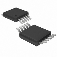
LTC3411EMS#TRPBF Linear Technology, LTC3411EMS#TRPBF Datasheet - Page 4

LTC3411EMS#TRPBF
Manufacturer Part Number
LTC3411EMS#TRPBF
Description
IC CONV DC/DC SYNC STPDWN 10MSOP
Manufacturer
Linear Technology
Type
Step-Down (Buck)r
Datasheet
1.LTC3411EDDPBF.pdf
(24 pages)
Specifications of LTC3411EMS#TRPBF
Internal Switch(s)
Yes
Synchronous Rectifier
Yes
Number Of Outputs
1
Voltage - Output
0.8 ~ 5 V
Current - Output
1.25A
Frequency - Switching
1MHz
Voltage - Input
2.63 ~ 5.5 V
Operating Temperature
-40°C ~ 85°C
Mounting Type
Surface Mount
Package / Case
10-MSOP, Micro10™, 10-uMAX, 10-uSOP
Lead Free Status / RoHS Status
Lead free / RoHS Compliant
Power - Output
-
Available stocks
Company
Part Number
Manufacturer
Quantity
Price
PIN FUNCTIONS
LTC3411
SHDN/R
Resistor Pin. The oscillator frequency is programmed by
connecting a resistor from this pin to ground. Forcing
this pin to SV
shutdown all functions are disabled.
SYNC/MODE (Pin 2): Combination Mode Selection and
Oscillator Synchronization Pin. This pin controls the op-
eration of the device. When tied to SV
Mode operation or pulse skipping mode is selected,
respectively. If this pin is held at half of SV
continuous mode is selected. The oscillation frequency
can be syncronized to an external oscillator applied to
this pin. When synchronized to an external clock pulse
skip mode is selected.
SGND (Pin 3): The Signal Ground Pin. All small signal
components and compensation components should be
connected to this ground (see Board Layout Consider-
ations).
SW (Pin 4): The Switch Node Connection to the Inductor.
This pin swings from PV
4
T
(Pin 1): Combination Shutdown and Timing
IN
causes the device to be shut down. In
IN
to PGND.
IN
or SGND, Burst
IN
, the forced
PGND (Pin 5): Main Power Ground Pin. Connect to the
(–) terminal of C
PV
to PGND.
SV
is powered from this pin. Must be closely decoupled to
SGND. SV
PGOOD (Pin 8): The Power Good Pin. This common drain
logic output is pulled to SGND when the output voltage is
not within ±7.5% of regulation.
V
ternal resistive divider across the output. Nominal voltage
for this pin is 0.8V.
I
current comparator threshold increases with this control
voltage. Nominal voltage range for this pin is 0V to 1.5V.
TH
FB
IN
IN
(Pin 10): Error Amplifi er Compensation Point. The
(Pin 9): Receives the feedback voltage from the ex-
(Pin 6): Main Supply Pin. Must be closely decoupled
(Pin 7): The Signal Power Pin. All active circuitry
IN
must be greater than or equal to PV
OUT
, and (–) terminal of C
IN
.
IN
.
3411fb


