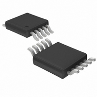
LTC1871IMS-7#TRPBF Linear Technology, LTC1871IMS-7#TRPBF Datasheet - Page 13

LTC1871IMS-7#TRPBF
Manufacturer Part Number
LTC1871IMS-7#TRPBF
Description
IC CONTRLR CURRENT MODE 10-MSOP
Manufacturer
Linear Technology
Type
Step-Up (Boost), Flyback, Sepicr
Datasheet
1.LTC1871EMS-7.pdf
(32 pages)
Specifications of LTC1871IMS-7#TRPBF
Internal Switch(s)
No
Synchronous Rectifier
No
Number Of Outputs
1
Voltage - Output
1.23 ~ 36 V
Current - Output
50mA
Frequency - Switching
50kHz ~ 1MHz
Voltage - Input
6 ~ 36 V
Operating Temperature
-40°C ~ 125°C
Mounting Type
Surface Mount
Package / Case
10-MSOP, Micro10™, 10-uMAX, 10-uSOP
Lead Free Status / RoHS Status
Lead free / RoHS Compliant
Power - Output
-
Available stocks
Company
Part Number
Manufacturer
Quantity
Price
APPLICATIONS INFORMATION
Application Circuits
A basic LTC1871-7 application circuit is shown in Figure 9.
External component selection is driven by the characteris-
tics of the load and the input supply. The fi rst topology to
be analyzed will be the boost converter, followed by SEPIC
(single-ended primary inductance converter).
Boost Converter: Duty Cycle Considerations
For a boost converter operating in a continuous conduction
mode (CCM), the duty cycle of the main switch is:
where V
converters where the input voltage is close to the output
voltage, the duty cycle is low and for converters that develop
a high output voltage from a low voltage input supply,
the duty cycle is high. The maximum output voltage for a
boost converter operating in CCM is:
D =
V
O(MAX)
D
V
O
is the forward voltage of the boost diode. For
V
+ V
=
O
(
+ V
1– D
D
V
IN(MIN)
– V
C
100pF
D
C2
MAX
IN
C
C
C
C
IN1
IN2
OUT1
OUT2
R
24k
:
:
)
C
C
2.2nF
: SANYO 100CV68FS
: TDK C5750X5R1H106M
C1
– V
SANYO 50MV560AXL (*RECOMMENDED FOR LAB EVALUATION
FOR SUPPLY LEAD LENGTHS GREATER THAN A FEW INCHES)
TDK C5750X5R1H106M
D
Figure 9. A High Effi ciency 42V, 1.5A Automotive Boost Converter
R
100k
1%
T
1
2
3
4
5
R3
1M
RUN
I
FB
FREQ
MODE/SYNC
TH
R1
12.4k
1%
f = 250kHz
LTC1871-7
412k
1%
R2
INTV
SENSE
GATE
GND
V
CC
IN
10
9
8
7
6
The maximum duty cycle capability of the LTC1871-7 is
typically 92%. This allows the user to obtain high output
voltages from low input supply voltages.
Boost Converter: The Peak and Average Input Currents
The control circuit in the LTC1871-7 is measuring the input
current typically using a sense resistor in the MOSFET
source, so the output current needs to be refl ected back
to the input in order to dimension the power MOSFET
properly. Based on the fact that, ideally, the output power
is equal to the input power, the maximum average input
current is:
The maximum duty cycle, D
minimum V
The peak input current is:
C
4.7μF
X5R
VCC
I
I
IN(MAX)
IN(PEAK)
C
10μF
50V
X5R
×2
IN2
D1: DIODES INC B360B
L1: COOPER DR127-6R8
M1: SILICONIX/VISHAY Si7370DP
=
IN
= 1+
M1
L1
6.8μH
R
0.005Ω
1W
1– D
.
SENSE
I
O(MAX)
D1
MAX
+
2
18717 F09
•
C
560μF
50V
IN1
1– D
C
10μF
50V
X5R
×2
I
*
O(MAX)
OUT2
MAX
MAX
+
, should be calculated at
C
68μF
100V
×2
OUT1
LTC1871-7
V
8V TO 28V
V
42V
1.5A
IN
GND
OUT
13
18717fc


