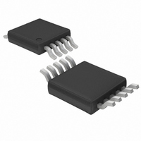
LTC1871IMS-7#TRPBF Linear Technology, LTC1871IMS-7#TRPBF Datasheet - Page 19

LTC1871IMS-7#TRPBF
Manufacturer Part Number
LTC1871IMS-7#TRPBF
Description
IC CONTRLR CURRENT MODE 10-MSOP
Manufacturer
Linear Technology
Type
Step-Up (Boost), Flyback, Sepicr
Datasheet
1.LTC1871EMS-7.pdf
(32 pages)
Specifications of LTC1871IMS-7#TRPBF
Internal Switch(s)
No
Synchronous Rectifier
No
Number Of Outputs
1
Voltage - Output
1.23 ~ 36 V
Current - Output
50mA
Frequency - Switching
50kHz ~ 1MHz
Voltage - Input
6 ~ 36 V
Operating Temperature
-40°C ~ 125°C
Mounting Type
Surface Mount
Package / Case
10-MSOP, Micro10™, 10-uMAX, 10-uSOP
Lead Free Status / RoHS Status
Lead free / RoHS Compliant
Power - Output
-
Available stocks
Company
Part Number
Manufacturer
Quantity
Price
APPLICATIONS INFORMATION
During this inductor charging interval, the output capacitor
must supply the load current and a signifi cant droop in
the output voltage can occur. Generally, it is a good idea
to choose a value of inductor ΔI
of I
of the output capacitor or disable Burst Mode operation
using the MODE/SYNC pin.
Burst Mode operation can be defeated by connecting the
MODE/SYNC pin to a high logic-level voltage (either with
a control input or by connecting this pin to INTV
this mode, the burst clamp is removed, and the chip can
operate at constant frequency from continuous conduction
mode (CCM) at full load, down into deep discontinuous
conduction mode (DCM) at light load. Prior to skipping
pulses at very light load (i.e., <5% of full load), the control-
ler will operate with a minimum switch on-time in DCM.
Pulse skipping prevents a loss of control of the output at
very light loads and reduces output voltage ripple.
Effi ciency Considerations
The effi ciency of a switching regulator is equal to the out-
put power divided by the input power (¥100%). Percent
effi ciency can be expressed as:
where L1, L2, etc. are the individual loss components as a
percentage of the input power. It is often useful to analyze
individual losses to determine what is limiting the effi ciency
and which change would produce the most improvement.
Although all dissipative elements in the circuit produce
losses, four main sources usually account for the majority
of the losses in LTC1871-7 application circuits:
1. The supply current into V
% Effi ciency = 100% – (L1 + L2 + L3 + …),
of the DC supply current I
acteristics) and the MOSFET driver and control currents.
The DC supply current into the V
650μA and represents a small power loss (much less
than 1%) that increases with V
results from switching the gate capacitance of the power
MOSFET; this current is typically much larger than the
DC current. Each time the MOSFET is switched on and
then off, a packet of gate charge Q
IN(MAX)
. The alternative is to either increase the value
IN
Q
(given in the Electrical Char-
. The V
L
between 25% and 40%
IN
IN
IN
G
pin is typically about
. The driver current
is transferred from
current is the sum
CC
). In
2. Power MOSFET switching and conduction losses:
3. The I
4. The losses in the inductor are simply the DC input cur-
5. Losses in the boost diode. The power dissipation in the
6. Other losses, including C
INTV
must be supplied to the INTV
V
CCM:
almost by inspection.
rent squared times the winding resistance. Expressing
this loss as a function of the output current yields:
boost diode is:
The boost diode can be a major source of power loss
in a boost converter. For 13.2V input, 42V output at
1.5A example given in Figure 9, a Schottky diode with
a 0.4V forward voltage would dissipate 600mW, which
represents about 1% of the input power. Diode losses
can become signifi cant at low output voltages where
the forward voltage is a signifi cant percentage of the
output voltage.
inductor core losses, generally account for less than
2% of the total losses.
IN
I
P
P
P
P
P
Q(TOT)
pin by an external supply. If the IC is operating in
IC
FET
R(SENSE)
R(WINDING)
DIODE
CC
2
R losses in the sense resistor can be calculated
= V
to ground. The resulting dQ/dt is a current that
+ k • V
=
IN
≈ I
= I
1– D
I
• (I
O(MAX)
Q
O(MAX)
=
O
= f • Q
=
Q
2
MAX
1– D
+ f • Q
•
I
O(MAX)
1– D
1– D
I
I
O(MAX)
• V
O(MAX)
G
MAX
2
D
MAX
G
MAX
• R
)
IN
DS(ON)
and C
2
• C
• R
CC
2
RSS
• R
SENSE
capacitor through the
O
LTC1871-7
• D
W
ESR dissipation and
• f
MAX
• D
•
MAX
T
19
18717fc


