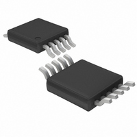
LTC1871IMS-7#TRPBF Linear Technology, LTC1871IMS-7#TRPBF Datasheet - Page 22

LTC1871IMS-7#TRPBF
Manufacturer Part Number
LTC1871IMS-7#TRPBF
Description
IC CONTRLR CURRENT MODE 10-MSOP
Manufacturer
Linear Technology
Type
Step-Up (Boost), Flyback, Sepicr
Datasheet
1.LTC1871EMS-7.pdf
(32 pages)
Specifications of LTC1871IMS-7#TRPBF
Internal Switch(s)
No
Synchronous Rectifier
No
Number Of Outputs
1
Voltage - Output
1.23 ~ 36 V
Current - Output
50mA
Frequency - Switching
50kHz ~ 1MHz
Voltage - Input
6 ~ 36 V
Operating Temperature
-40°C ~ 125°C
Mounting Type
Surface Mount
Package / Case
10-MSOP, Micro10™, 10-uMAX, 10-uSOP
Lead Free Status / RoHS Status
Lead free / RoHS Compliant
Power - Output
-
Available stocks
Company
Part Number
Manufacturer
Quantity
Price
LTC1871-7
APPLICATIONS INFORMATION
PC Board Layout Checklist
1. In order to minimize switching noise and improve out-
put load regulation, the GND pin of the LTC1871-7 should
be connected directly to 1) the negative terminal of the
INTV
the output decoupling capacitors, 3) the bottom terminal
of the sense resistor, 4) the negative terminal of the input
capacitor and 5) at least one via to the ground plane
immediately adjacent to Pin 6. The ground trace on the
top layer of the PC board should be as wide and short as
possible to minimize series resistance and inductance.
2. Beware of ground loops in multiple layer PC boards. Try
to maintain one central ground node on the board and use
the input capacitor to avoid excess input ripple for high
output current power supplies. If the ground plane is to
be used for high DC currents, choose a path away from
the small-signal components.
3. Place the C
INTV
carries high di/dt MOSFET gate drive currents. A low ESR
and ESL 4.7μF ceramic capacitor works well here.
4. The high di/dt loop from the bottom terminal of the
output capacitor, through the power MOSFET, through
the boost diode and back through the output capacitors
should be kept as tight as possible to reduce inductive
22
VOLTAGE
MOSFET
20V/DIV
1V/DIV
1A/DIV
DRAIN
CC
CC
V
OUT
I
L
decoupling capacitor, 2) the negative terminal of
and GND pins on the IC package. This capacitor
V
I
V
D = 27%
OUT
Figure 16. Switching Waveforms for the
Converter in Figure 9 at Maximum V
IN
OUT
= 28V
= 0.5A
= 42V
VCC
capacitor immediately adjacent to the
1μs/DIV
IN
(28V)
18717 F16
ringing. Excess inductance can cause increased stress on
the power MOSFET and increase HF noise on the output.
If low ESR ceramic capacitors are used on the output to
reduce output noise, place these capacitors close to the
boost diode in order to keep the series inductance to a
minimum.
5. Check the stress on the power MOSFET by measur-
ing its drain-to-source voltage directly across the device
terminals (reference the ground of a single scope probe
directly to the source pad on the PC board). Beware of
inductive ringing which can exceed the maximum speci-
fi ed voltage rating of the MOSFET. If this ringing cannot be
avoided and exceeds the maximum rating of the device,
either choose a higher voltage device or specify an ava-
lanche-rated power MOSFET. Not all MOSFETs are created
equal (some are more equal than others).
6. Place the small-signal components away from high fre-
quency switching nodes. In the layout shown in Figure 18,
all of the small-signal components have been placed on
one side of the IC and all of the power components have
been placed on the other. This also allows the use of a
pseudo-Kelvin connection for the signal ground, where
high di/dt gate driver currents fl ow out of the IC ground
pin in one direction (to the bottom plate of the INTV
decoupling capacitor) and small-signal currents fl ow in
the other direction.
Figure 17. Effi ciency vs Load Current and Input Voltage
for the Converter in Figure 9
100
95
90
85
80
75
0.001
V
V
V
0.01
IN
IN
IN
= 8V
= 12V
= 28V
I
LOAD
0.1
(mA)
1
18717 F17
10
18717fc
CC


