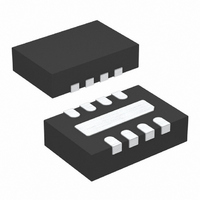
LTC3642IDD-5#TRPBF Linear Technology, LTC3642IDD-5#TRPBF Datasheet - Page 12

LTC3642IDD-5#TRPBF
Manufacturer Part Number
LTC3642IDD-5#TRPBF
Description
IC DC/DC CONV HE/HV 5V 8-DFN
Manufacturer
Linear Technology
Type
Step-Down (Buck)r
Datasheet
1.LTC3642EMS8EPBF.pdf
(22 pages)
Specifications of LTC3642IDD-5#TRPBF
Internal Switch(s)
Yes
Synchronous Rectifier
Yes
Number Of Outputs
1
Voltage - Output
5V
Current - Output
50mA
Voltage - Input
4.5 ~ 45 V
Operating Temperature
-40°C ~ 125°C
Mounting Type
Surface Mount
Package / Case
8-DFN
Lead Free Status / RoHS Status
Lead free / RoHS Compliant
Power - Output
-
Frequency - Switching
-
Available stocks
Company
Part Number
Manufacturer
Quantity
Price
APPLICATIONS INFORMATION
LTC3642
This formula has a maximum at V
I
commonly used for design because even significant
deviations do not offer much relief. Note that ripple current
ratings from capacitor manufacturers are often based
only on 2000 hours of life which makes it advisable to
further derate the capacitor, or choose a capacitor rated
at a higher temperature than required. Several capacitors
may also be paralleled to meet size or height requirements
in the design.
The output capacitor, C
current and stores energy to satisfy the load current when
the LTC3642 is in sleep. The output ripple has a lower limit
of V
back comparator. The time delay of the comparator adds
an additional ripple voltage that is a function of the load
current. During this delay time, the LTC3642 continues to
switch and supply current to the output. The output ripple
can be approximated by:
The output ripple is a maximum at no load and approaches
lower limit of V
capacitor C
mum load current.
The value of the output capacitor must be large enough
to accept the energy stored in the inductor without a large
change in output voltage. Setting this voltage step equal to
1% of the output voltage, the output capacitor must be:
Typically, a capacitor that satisfies the voltage ripple
requirement is adequate to filter the inductor ripple. To
avoid overheating, the output capacitor must also be sized
to handle the ripple current generated by the inductor. The
worst-case ripple current in the output capacitor is given
by I
may be needed to meet the ESR and RMS current handling
requirements.
12
RMS
C
ΔV
OUT
RMS
OUT
= I
OUT
/160 due to the 5mV typical hysteresis of the feed-
OUT
= I
> 50 • L •
≈
OUT
PEAK
/2. This simple worst-case condition is
I
PEAK
to limit the output voltage ripple at mini-
2
/2. Multiple capacitors placed in parallel
OUT
/160 at full load. Choose the output
I
– I
V
PEAK
OUT
LOAD
OUT
2
, filters the inductor’s ripple
4 • 10
C
OUT
– 6
IN
+
= 2V
V
160
OUT
OUT
, where
Dry tantalum, special polymer, aluminum electrolytic,
and ceramic capacitors are all available in surface mount
packages. Special polymer capacitors offer very low ESR
but have lower capacitance density than other types.
Tantalum capacitors have the highest capacitance density
but it is important only to use types that have been surge
tested for use in switching power supplies. Aluminum
electrolytic capacitors have significantly higher ESR but
can be used in cost-sensitive applications provided that
consideration is given to ripple current ratings and long-
term reliability. Ceramic capacitors have excellent low ESR
characteristics but can have high voltage coefficient and
audible piezoelectric effects. The high quality factor (Q)
of ceramic capacitors in series with trace inductance can
also lead to significant ringing.
Using Ceramic Input and Output Capacitors
Higher value, lower cost ceramic capacitors are now be-
coming available in smaller case sizes. Their high ripple
current, high voltage rating and low ESR make them ideal
for switching regulator applications. However, care must
be taken when these capacitors are used at the input and
output. When a ceramic capacitor is used at the input and
the power is supplied by a wall adapter through long wires,
a load step at the output can induce ringing at the input,
V
mistaken as loop instability. At worst, a sudden inrush
of current through the long wires can potentially cause a
voltage spike at V
For applications with inductive source impedance, such
as a long wire, a series RC network may be required in
parallel with C
Figure 5 shows this circuit and the typical values required
to dampen the ringing.
IN
. At best, this ringing can couple to the output and be
Figure 5. Series RC to Reduce V
IN
to dampen the ringing of the input supply.
L
IN
IN
large enough to damage the LTC3642.
R =
4 • C
IN
L
C
IN
IN
C
IN
V
IN
LTC3642
IN
Ringing
3642 F05
3642fc


