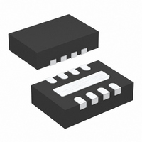
LTC3642IDD-5#TRPBF Linear Technology, LTC3642IDD-5#TRPBF Datasheet - Page 3

LTC3642IDD-5#TRPBF
Manufacturer Part Number
LTC3642IDD-5#TRPBF
Description
IC DC/DC CONV HE/HV 5V 8-DFN
Manufacturer
Linear Technology
Type
Step-Down (Buck)r
Datasheet
1.LTC3642EMS8EPBF.pdf
(22 pages)
Specifications of LTC3642IDD-5#TRPBF
Internal Switch(s)
Yes
Synchronous Rectifier
Yes
Number Of Outputs
1
Voltage - Output
5V
Current - Output
50mA
Voltage - Input
4.5 ~ 45 V
Operating Temperature
-40°C ~ 125°C
Mounting Type
Surface Mount
Package / Case
8-DFN
Lead Free Status / RoHS Status
Lead free / RoHS Compliant
Power - Output
-
Frequency - Switching
-
Available stocks
Company
Part Number
Manufacturer
Quantity
Price
ELECTRICAL CHARACTERISTICS
junction temperature range, otherwise specifications are for T
SYMBOL
Input Supply (V
V
UVLO
OVLO
I
Output Supply (V
V
V
V
I
∆V
Operation
V
I
V
I
I
t
I
R
Note 1: Stresses beyond those listed under Absolute Maximum Ratings
may cause permanent damage to the device. Exposure to any Absolute
Maximum Rating condition for extended periods may affect device
reliability and lifetime.
Note 2: The LTC3642 is tested under pulsed load conditions such that T
LTC3642E is guaranteed to meet specifications from 0°C to 85°C junction
temperature. Specifications over the –40°C to 125°C operating junction
temperature range are assured by design, characterization and correlation
with statistical process controls. The LTC3642I is guaranteed over the
full –40°C to 125°C operating junction temperature range. Note that the
Q
FB
RUN
HYST
SS
INTSS
PEAK
IN
OUT
FB
HYST
RUN
HYSTL
ON
LINEREG
IN
PARAMETER
Input Voltage Operating Range
V
V
DC Supply Current (Note 3)
Output Voltage Trip Thresholds
Feedback Comparator Trip Voltage
Feedback Comparator Hysteresis Voltage
Feedback Pin Current
Feedback Voltage Line Regulation
Run Pin Threshold Voltage
Run Pin Leakage Current
Hysteresis Pin Voltage Low
Hysteresis Pin Leakage Current
Soft-Start Pin Pull-Up Current
Internal Soft-Start Time
Peak Current Trip Threshold
Power Switch On-Resistance
OUT
)
IN
IN
Active Mode
Sleep Mode
Shutdown Mode
Top Switch
Bottom Switch
Undervoltage Lockout
Overvoltage Lockout
/V
FB
)
CONDITIONS
V
V
Hysteresis
V
V
Hysteresis
V
LTC3642-3.3V, V
LTC3642-3.3V, V
LTC3642-5V, V
LTC3642-5V, V
V
Adjustable Output Version, V
V
LTC3642-5, V
RUN Rising
RUN Falling
Hysteresis
RUN = 1.3V
RUN < 1V, I
V
V
SS Pin Floating
I
500k Resistor from I
I
I
I
SET
SET
SW
SW
IN
IN
IN
IN
RUN
FB
IN
HYST
SS
Rising
Falling
Rising
Falling
= 4.5V to 45V
Rising
= –25mA
= 25mA
< 1.5V
Floating
Shorted to GND
= 0V
= 1.3V
The
J
≈ T
A
HYST
l
A
= 25°C (Note 2). V
IN
.
OUT
OUT
denotes the specifications which apply over the full operating
= 6V to 45V
OUT
OUT
= 1mA
Rising
Falling
maximum ambient temperature consistent with these specifications is
determined by specific operating conditions in conjunction with board
layout, the rated package thermal impedance and other environmental
factors. The junction temperature (T
temperature (T
the formula:
Note 3: Dynamic supply current is higher due to the gate charge being
delivered at the switching frequency. See Applications Information.
Rising
Falling
SET
T
impedance.
to GND
J
= T
FB
A
= 1V
+ (P
IN
A
D
, in °C) and power dissipation (P
= 10V, unless otherwise noted.
• θ
JA
), where θ
l
l
l
l
l
l
l
l
l
3.260
3.240
4.940
4.910
0.792
3.80
3.75
1.17
1.06
MIN
–10
–10
–10
100
4.5
4.5
47
45
20
3
JA
(in °C/W) is the package thermal
J
, in °C) is calculated from the ambient
3.310
3.290
5.015
4.985
0.800
0.001
4.15
4.00
1.21
1.10
0.07
0.75
TYP
150
125
110
115
5.5
3.0
1.5
50
48
12
55
25
2
3
5
0
0
0
D
, in Watts) according to
LTC3642
3.360
3.340
5.090
5.060
0.808
MAX
4.50
4.35
1.25
1.14
220
130
0.1
6.5
45
52
50
22
10
10
10
32
6
7
UNITS
3642fc
3
%/V
mV
mV
mV
mA
mA
mA
ms
µA
µA
µA
nA
nA
nA
µA
Ω
Ω
V
V
V
V
V
V
V
V
V
V
V
V
V
V


