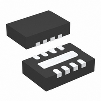
LTC3642IDD-5#TRPBF Linear Technology, LTC3642IDD-5#TRPBF Datasheet - Page 16

LTC3642IDD-5#TRPBF
Manufacturer Part Number
LTC3642IDD-5#TRPBF
Description
IC DC/DC CONV HE/HV 5V 8-DFN
Manufacturer
Linear Technology
Type
Step-Down (Buck)r
Datasheet
1.LTC3642EMS8EPBF.pdf
(22 pages)
Specifications of LTC3642IDD-5#TRPBF
Internal Switch(s)
Yes
Synchronous Rectifier
Yes
Number Of Outputs
1
Voltage - Output
5V
Current - Output
50mA
Voltage - Input
4.5 ~ 45 V
Operating Temperature
-40°C ~ 125°C
Mounting Type
Surface Mount
Package / Case
8-DFN
Lead Free Status / RoHS Status
Lead free / RoHS Compliant
Power - Output
-
Frequency - Switching
-
Available stocks
Company
Part Number
Manufacturer
Quantity
Price
APPLICATIONS INFORMATION
LTC3642
The undervoltage lockout requirement on V
satisfied with a resistive divider from V
HYST pins. Choose R1 = 2M and calculate R2 and R3 as
follows:
Choose standard values for R2 = 226k and R3 = 91k. The
I
mum peak current (115mA). Figure 9 shows a complete
schematic for this design example.
PC Board Layout Checklist
When laying out the printed circuit board, the following
checklist should be used to ensure proper operation of
the LTC3642. Check the following in your layout:
1. Large switched currents flow in the power switches
2. Connect the (+) terminal of the input capacitor, C
16
SET
and input capacitor. The loop formed by these compo-
nents should be as small as possible. A ground plane
is recommended to minimize ground impedance.
close as possible to the V
the AC current into the internal power MOSFETs.
R2 =
R3 =
pin should be left open in this example to select maxi-
24V
V
IN
Figure 9. 24V to 3.3V, 50mA Regulator at 250kHz
V
V
IN(RISING)
IN(FALLING)
1µF
1.21V
1.1V
2M
226k
91k
– 1.21V
– 1.1V
V
RUN
HYST
IN
LTC3642
GND
IN
• R1– R2 = 90.8k
• R1= 224k
I
SW
V
pin. This capacitor provides
SET
SS
FB
100µH
IN
750k
240k
to the RUN and
3642 F09
10µF
IN
V
3.3V
50mA
OUT
can be
IN
, as
3. Keep the switching node, SW, away from all sensitive
4. Flood all unused area on all layers with copper. Flooding
V
small signal nodes. The rapid transitions on the switching
node can couple to high impedance nodes, in particular
V
with copper will reduce the temperature rise of power
components. You can connect the copper areas to any
DC net (V
system).
IN
FB
V
IN
, and create increased output ripple.
R
C
SET
VIAS TO GROUND PLANE
VIAS TO INPUT SUPPLY (V
OUTLINE OF LOCAL GROUND PLANE
IN
IN
, V
C
SS
C
Figure 10. Layout Example
OUT
SS
2
5
7
4
V
RUN
HYST
SS
, GND or any other DC rail in your
IN
LTC3642
GND
L1
8, 9
C
GND
IN
I
SW
V
SET
FB
IN
)
1
6
3
C
OUT
L1
R
SET
R1
R2
R1
3642 F10a
3642 F10b
R2
C
V
OUT
OUT
V
OUT
3642fc


