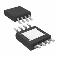
LTC3642IMS8E-5#TRPBF Linear Technology, LTC3642IMS8E-5#TRPBF Datasheet - Page 15

LTC3642IMS8E-5#TRPBF
Manufacturer Part Number
LTC3642IMS8E-5#TRPBF
Description
IC DC/DC CONV HE/HV 5V 8-MSOP
Manufacturer
Linear Technology
Type
Step-Down (Buck)r
Datasheet
1.LTC3642EMS8EPBF.pdf
(22 pages)
Specifications of LTC3642IMS8E-5#TRPBF
Internal Switch(s)
Yes
Synchronous Rectifier
Yes
Number Of Outputs
1
Voltage - Output
5V
Current - Output
50mA
Voltage - Input
4.5 ~ 45 V
Operating Temperature
-40°C ~ 125°C
Mounting Type
Surface Mount
Package / Case
8-MSOP Exposed Pad, 8-HMSOP, 8-eMSOP
Lead Free Status / RoHS Status
Lead free / RoHS Compliant
Power - Output
-
Frequency - Switching
-
Available stocks
Company
Part Number
Manufacturer
Quantity
Price
APPLICATIONS INFORMATION
2. I
Thermal Considerations
The LTC3642 does not dissipate much heat due to its high
efficiency and low peak current level. Even in worst-case
conditions (high ambient temperature, maximum peak
current and high duty cycle), the junction temperature will
exceed ambient temperature by only a few degrees.
Design Example
As a design example, consider using the LTC3642 in an
application with the following specifications: V
V
sume for this example that switching should start when
V
than 8V.
OUT
IN
The gate charge current results from switching the gate
capacitance of the internal power MOSFET switches.
Each time the gate is switched from high to low to
high again, a packet of charge, dQ, moves from V
ground. The resulting dQ/dt is the current out of V
that is typically larger than the DC bias current.
internal switches, R
switching, the average output current flowing through
the inductor is “chopped” between the high side PMOS
switch and the low side NMOS switch. Thus, the series
resistance looking back into the switch pin is a function
of the top and bottom switch R
duty cycle (DC = V
The R
be obtained from the Typical Performance Characteris-
tics curves. Thus, to obtain the I
R
average output current:
Other losses, including C
losses and inductor core losses, generally account for
less than 2% of the total power loss.
2
is greater than 12V and should stop when V
SW
R losses are calculated from the resistances of the
R
I
= 3.3V, I
2
SW
R Loss = I
to R
DS(ON)
= (R
L
and multiply the result by the square of the
OUT
DS(ON)TOP
for both the top and bottom MOSFETs can
O
= 50mA, f = 250kHz. Furthermore, as-
2
(R
OUT
SW
SW
)DC + (R
/V
, and external inductor R
+ R
IN
IN
) as follows:
L
)
and C
DS(ON)BOT
DS(ON)
2
R losses, simply add
OUT
ESR dissipative
values and the
)(1 – DC)
IN
IN
L
. When
= 24V,
is less
IN
to
IN
First, calculate the inductor value that gives the required
switching frequency:
Next, verify that this value meets the L
For this input voltage and peak current, the minimum
inductor value is:
Therefore, the minimum inductor requirement is satisfied,
and the 100μH inductor value may be used.
Next, C
be size for a current rating of at least:
Due to the low peak current of the LTC3642, decoupling
the V
applications.
C
requirement. For a 1.5% (50mV) output voltage ripple at
no load, C
A 7.8µF capacitor gives this typical output voltage ripple at
no load. Choose a 10µF capacitor as a standard value.
The output voltage can now be programmed by choosing
the values of R1 and R2. Choose R2 = 240k and calculate
R1 as:
OUT
I
L =
L
C
R1=
RMS
MIN
OUT
IN
will be selected based on the output voltage ripple
Ê
Ë Á
IN
supply with a 1µF capacitor is adequate for most
250kHz • 115mA
= 50mA •
=
=
and C
0.8V
V
OUT
OUT
24V • 100ns
115 mA • 4 • 10
2 50mV –
115mA
can be calculated from:
3.3V
OUT
– 1
• R2 = 750k
are selected. For this design, C
3.3V
24V
3.3V
160
≅ 22µH
•
ˆ
¯ ˜
–6
• 1–
3.3V
24V
Ê
Ë Á
3.3V
– 1 ≅ 18mA
24V
ˆ
¯ ˜
LTC3642
MIN
@ 100µH
requirement.
RMS
IN
15
should
3642fc


