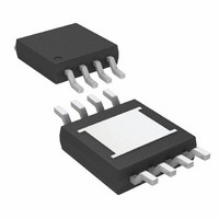
LTC3642IMS8E-5#TRPBF Linear Technology, LTC3642IMS8E-5#TRPBF Datasheet

LTC3642IMS8E-5#TRPBF
Specifications of LTC3642IMS8E-5#TRPBF
Available stocks
Related parts for LTC3642IMS8E-5#TRPBF
LTC3642IMS8E-5#TRPBF Summary of contents
Page 1
... The LTC3642 is available in the thermally enhanced 3mm × 3mm DFN and MS8E packages. L, LT, LTC, LTM, Burst Mode, Linear Technology, and the Linear logo are registered trademarks and ThinSOT is a trademark of Linear Technology Corporation. All other trademarks are the property of their respective owners. ...
Page 2
... LEAD FREE FINISH TAPE AND REEL LTC3642EMS8E#PBF LTC3642EMS8E#TRPBF LTC3642EMS8E-3.3#PBF LTC3642EMS8E-3.3#TRPBF LTC3642EMS8E-5#PBF LTC3642EMS8E-5#TRPBF LTC3642IMS8E#PBF LTC3642IMS8E#TRPBF LTC3642IMS8E-3.3#PBF LTC3642IMS8E-3.3#TRPBF LTC3642IMS8E-5#PBF LTC3642IMS8E-5#TRPBF LTC3642EDD#PBF LTC3642EDD#TRPBF LTC3642EDD-3.3#PBF LTC3642EDD-3.3#TRPBF LTC3642EDD-5#PBF LTC3642EDD-5#TRPBF LTC3642IDD#PBF LTC3642IDD#TRPBF LTC3642IDD-3.3#PBF LTC3642IDD-3.3#TRPBF LTC3642IDD-5#PBF LTC3642IDD-5#TRPBF Consult LTC Marketing for parts specified with wider operating temperature ranges. *The temperature grade is identified by a label on the shipping container. ...
Page 3
ELECTRICAL CHARACTERISTICS junction temperature range, otherwise specifications are for T SYMBOL PARAMETER Input Supply ( Input Voltage Operating Range IN UVLO V Undervoltage Lockout IN OVLO V Overvoltage Lockout Supply Current (Note 3) Q ...
Page 4
LTC3642 TYPICAL PERFORMANCE CHARACTERISTICS Efficiency vs Load Current 100 FIGURE 11 CIRCUIT I OPEN 95 SET V = 10V OUT 15V 45V 24V IN 75 ...
Page 5
TYPICAL PERFORMANCE CHARACTERISTICS Switch On-Resistance vs Input Voltage 4.5 4.0 3.5 TOP 3.0 2.5 2.0 BOTTOM 1.5 1.0 0 INPUT VOLTAGE (V) 3642 G10 Efficiency vs Input Voltage 95 FIGURE 11 CIRCUIT I OPEN ...
Page 6
LTC3642 PIN FUNCTIONS SW (Pin 1): Switch Node Connection to Inductor. This pin connects to the drains of the internal power MOSFET switches. V (Pin 2): Main Supply Pin. A ceramic bypass capacitor IN should be tied between this pin ...
Page 7
BLOCK DIAGRAM 1µA I SET 3 RUN + 5 – 1.2V HYST 7 GND GND 8 9 PEAK CURRENT – COMPARATOR + LOGIC AND SHOOT- THROUGH PREVENTION + REVERSE CURRENT – COMPARATOR VOLTAGE REFERENCE FEEDBACK + COMPARATOR 0.800V + – ...
Page 8
LTC3642 OPERATION (Refer to Block Diagram) The LTC3642 is a step-down DC/DC converter with internal power switches that uses Burst Mode control, combining low quiescent current with high switching frequency, which results in high efficiency across a wide range of ...
Page 9
OPERATION (Refer to Block Diagram) inductor current from 25mA during its 1ms ramp time to the set peak current threshold. The external ramp on the SS pin does not limit the peak inductor current during start-up; however, placing a capacitor ...
Page 10
LTC3642 APPLICATIONS INFORMATION The basic LTC3642 application circuit is shown on the front page of this data sheet. External component selection is determined by the maximum load current requirement and begins with the selection of the peak current programming resistor, ...
Page 11
APPLICATIONS INFORMATION 700 OUT I OPEN SET L = 47µH 600 500 L = 68µH 400 L = 100µH 300 L = 150µH 200 L = 220µ 470µH 100 ...
Page 12
LTC3642 APPLICATIONS INFORMATION This formula has a maximum /2. This simple worst-case condition is RMS OUT commonly used for design because even significant deviations do not offer much relief. Note that ripple current ratings from ...
Page 13
APPLICATIONS INFORMATION Output Voltage Programming For the adjustable version, the output voltage is set by an external resistive divider according to the following equation: R1 0.8V • 1+ OUT R2 The resistive ...
Page 14
LTC3642 APPLICATIONS INFORMATION The minimum value of these thresholds is limited to the internal V UVLO thresholds that are shown in the Electri- IN cal Characteristics table. The current that flows through this divider will directly add to the shutdown, ...
Page 15
APPLICATIONS INFORMATION The gate charge current results from switching the gate capacitance of the internal power MOSFET switches. Each time the gate is switched from high to low to high again, a packet of charge, dQ, moves from V ground. ...
Page 16
LTC3642 APPLICATIONS INFORMATION The undervoltage lockout requirement on V satisfied with a resistive divider from V HYST pins. Choose and calculate R2 and R3 as follows: 1.21V R2 = • R1= 224k ...
Page 17
TYPICAL APPLICATIONS L1 220µ 45V C LTC3642 IN 4.7µF RUN V FB HYST I SS SET GND R SET C : TDK C5750X7R2A475MT AVX 1812D107MAT OUT L1: TDK SLF7045T-221MR33-PF Figure ...
Page 18
LTC3642 TYPICAL APPLICATIONS 45V High Efficiency 15V, 10mA Regulator L1 4700µ 15V TO 45V C LTC3642 IN 1µF RUN SET SS HYST GND C : AVX 18125C105KAT2A IN ...
Page 19
PACKAGE DESCRIPTION 3.5 ±0.05 1.65 ±0.05 2.10 ±0.05 (2 SIDES) 0.25 ± 0.05 RECOMMENDED SOLDER PAD PITCH AND DIMENSIONS APPLY SOLDER MASK TO AREAS THAT ARE NOT SOLDERED PIN 1 TOP MARK (NOTE 6) 0.200 REF DD Package 8-Lead Plastic ...
Page 20
LTC3642 PACKAGE DESCRIPTION 1.88 ± 0.102 (.074 ± .004) 5.23 (.206) MIN 0.42 ± 0.038 (.0165 ± .0015) TYP RECOMMENDED SOLDER PAD LAYOUT DETAIL “A” 0.254 (.010) GAUGE PLANE DETAIL “A” 0.18 (.007) NOTE: 1. DIMENSIONS IN MILLIMETER/(INCH) 2. DRAWING ...
Page 21
... DESCRIPTION B 6/10 Text updates in Description Updates to Absolute Maximum Ratings LTC3642IMS8E-3.3E#PBF changed to LTC3642IMS8E-3.3#PBF in Order Information Updates to Electrical Characteristics Updates to graphs G05, G06, G14, G16, G17 Updated description for Pins 8 and 9 in Pin Functions Text updates in Operation section Text updates in Applications Information section ...
Page 22
... MSOP8 OUT(MIN 1.25V 12µA, I < 1µA, OUT(MIN 0.8V 2.5mA, I < 10µA, OUT(MIN 1.25V 100µA, I < 1µA, OUT(MIN 1.2V 26µA, I < 1µA, OUT(MIN 0.78V 70µA, I < 1µA, OUT(MIN 1010 REV C • PRINTED IN USA LINEAR TECHNOLOGY CORPORA TION 2008 3642fc ...


