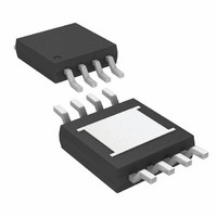
LTC3642IMS8E-5#TRPBF Linear Technology, LTC3642IMS8E-5#TRPBF Datasheet - Page 6

LTC3642IMS8E-5#TRPBF
Manufacturer Part Number
LTC3642IMS8E-5#TRPBF
Description
IC DC/DC CONV HE/HV 5V 8-MSOP
Manufacturer
Linear Technology
Type
Step-Down (Buck)r
Datasheet
1.LTC3642EMS8EPBF.pdf
(22 pages)
Specifications of LTC3642IMS8E-5#TRPBF
Internal Switch(s)
Yes
Synchronous Rectifier
Yes
Number Of Outputs
1
Voltage - Output
5V
Current - Output
50mA
Voltage - Input
4.5 ~ 45 V
Operating Temperature
-40°C ~ 125°C
Mounting Type
Surface Mount
Package / Case
8-MSOP Exposed Pad, 8-HMSOP, 8-eMSOP
Lead Free Status / RoHS Status
Lead free / RoHS Compliant
Power - Output
-
Frequency - Switching
-
Available stocks
Company
Part Number
Manufacturer
Quantity
Price
PIN FUNCTIONS
LTC3642
SW (Pin 1): Switch Node Connection to Inductor. This
pin connects to the drains of the internal power MOSFET
switches.
V
should be tied between this pin and GND (Pin 8).
I
pin to ground sets the peak current trip threshold. Leave
floating for the maximum peak current (115mA). Short
this pin to ground for the minimum peak current (25mA).
A 1µA current is sourced out of this pin.
SS (Pin 4): Soft-Start Control Input. A capacitor to ground
at this pin sets the ramp time to full current output dur-
ing start-up. A 5µA current is sourced out of this pin. If
left floating, the ramp time defaults to an internal 0.75ms
soft-start.
RUN (Pin 5): Run Control Input. A voltage on this pin
above 1.2V enables normal operation. Forcing this pin
below 0.7V shuts down the LTC3642, reducing quiescent
current to approximately 3µA.
6
SET
IN
(Pin 2): Main Supply Pin. A ceramic bypass capacitor
(Pin 3): Peak Current Set Input. A resistor from this
V
output versions, connect this pin to the output supply. For
the adjustable version, an external resistive divider should
be used to divide the output voltage down for comparison
to the 0.8V reference.
HYST (Pin 7): Run Hysteresis Open-Drain Logic Output.
This pin is pulled to ground when RUN (Pin 5) is below
1.2V. This pin can be used to adjust the RUN pin hysteresis.
See Applications Information.
GND (Pin 8, Exposed Pad Pin 9): Ground. The exposed
pad must be soldered to the printed circuit board ground
plane for optimal electrical and thermal performance.
OUT
/V
FB
(Pin 6): Output Voltage Feedback. For the fixed
3642fc


