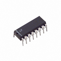
LTC1149CN-5 Linear Technology, LTC1149CN-5 Datasheet - Page 15

LTC1149CN-5
Manufacturer Part Number
LTC1149CN-5
Description
IC SW REG STEP-DOWN 5V 16-DIP
Manufacturer
Linear Technology
Type
Step-Down (Buck)r
Datasheet
1.LTC1149CNPBF.pdf
(20 pages)
Specifications of LTC1149CN-5
Internal Switch(s)
No
Synchronous Rectifier
Yes
Number Of Outputs
1
Voltage - Output
5V
Current - Output
50mA
Frequency - Switching
250kHz
Voltage - Input
0 ~ 48 V
Operating Temperature
0°C ~ 70°C
Mounting Type
Through Hole
Package / Case
16-DIP (0.300", 7.62mm)
Lead Free Status / RoHS Status
Contains lead / RoHS non-compliant
Power - Output
-
Available stocks
Company
Part Number
Manufacturer
Quantity
Price
Company:
Part Number:
LTC1149CN-5
Manufacturer:
LT
Quantity:
6 244
Part Number:
LTC1149CN-5#PBF
Manufacturer:
LINEAR/凌特
Quantity:
20 000
APPLICATIO S I FOR ATIO
4. Does the (+) plate of C
5. Is the V
6. Is the SHDN1 Pin 10 (fixed output versions only)
Troubleshooting Hints
Since efficiency is critical to LTC1149 series applications,
it is very important to verify that the circuit is functioning
in series with each sense lead to help decouple Pins 8
and 9. However, when these resistors are used, the
capacitor should be no larger than 1000pF.
P-channel MOSFET as closely as possible? An addi-
tional 0.1 F ceramic capacitor between V
ground may be required in some applications.
between Pin 5 of the LTC1149 and power ground? This
capacitor carries the MOSFET driver peak currents.
actively pulled to ground during normal operation? The
SHDN1 pin is high impedance and must not be allowed
to float. In adjustable versions, Pin 10 is the feedback
pin and is very sensitive to pickup from the switch node.
Care must be taken to isolate V
tive coupling of the inductor switch signal.
CC
decoupling capacitor connected closely
U U
1149 F08
C
T
IN
connect to the source of the
1k
1N4148
0.047 F
3300pF
Figure 8. LTC1149 Series Layout Diagram (see Layout Checklist)
FB
from possible capaci-
W
1
2
3
4
5
6
7
8
+
PGATE
V
V
PDRIVE
V
C
I
SENSE
1 F
TH
IN
CC
CC
T
IN
–
0.068 F
and power
BOLD LINES INDICATE HIGH CURRENT PATHS
U
SENSE
1000pF
NGATE
SHDN1
RGND
PGND
SGND
CAP
SD2
V
1N4148
FB
+
/
16
15
14
13
12
11
10
9
SHUTDOWN
correctly in both continuous and Burst Mode operation.
The waveform to monitor is the voltage on the timing
capacitor Pin 6.
In continuous mode (I
should be a sawtooth with a 0.9V
should never dip below 2V as shown in Figure 9a.
When load currents are low (I
operation should occur with the C
cally falling to ground as shown in Figure 9b.
If Pin 6 is observed falling to ground at high output
currents, it indicates poor decoupling or improper ground-
ing. Refer to the Board Layout Checklist.
P-CHANNEL
100pF
R1
R2
(a) CONTINUOUS MODE OPERATION
Figure 9. C
LTC1149-3.3/LTC1149-5
N-CHANNEL
+
(b) Burst Mode OPERATION
D1
L
C
LOAD
OUT
T
C
Pin 6 Waveforms
IN
R
SENSE
OUTPUT DIVIDER REQUIRED WITH
ADJUSTABLE VERSION ONLY
> I
BURST
LOAD
V
V
OUT
+
–
–
+
IN
T
P-P
pin waveform periodi-
< I
) the voltage on Pin 6
swing. This voltage
BURST
LTC1149
) Burst Mode
15
1149 F09
0V
0V
3.3V
3.3V


