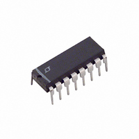
LTC1149CN-5 Linear Technology, LTC1149CN-5 Datasheet - Page 3

LTC1149CN-5
Manufacturer Part Number
LTC1149CN-5
Description
IC SW REG STEP-DOWN 5V 16-DIP
Manufacturer
Linear Technology
Type
Step-Down (Buck)r
Datasheet
1.LTC1149CNPBF.pdf
(20 pages)
Specifications of LTC1149CN-5
Internal Switch(s)
No
Synchronous Rectifier
Yes
Number Of Outputs
1
Voltage - Output
5V
Current - Output
50mA
Frequency - Switching
250kHz
Voltage - Input
0 ~ 48 V
Operating Temperature
0°C ~ 70°C
Mounting Type
Through Hole
Package / Case
16-DIP (0.300", 7.62mm)
Lead Free Status / RoHS Status
Contains lead / RoHS non-compliant
Power - Output
-
Available stocks
Company
Part Number
Manufacturer
Quantity
Price
Company:
Part Number:
LTC1149CN-5
Manufacturer:
LT
Quantity:
6 244
Part Number:
LTC1149CN-5#PBF
Manufacturer:
LINEAR/凌特
Quantity:
20 000
SYMBOL
V
V
V
I
I
t
t
ELECTRICAL C
– 40 C T
SYMBOL
V
V
I
V
V
V
t
The
temperature range.
Note 1: T
dissipation P
Note 2: Pin 10 is a shutdown pin on the LTC1149-3.3 and LTC1149-5
fixed output voltage versions and must be at ground potential for testing.
15
6
OFF
r
2
OFF
9
10
15
, t
10
OUT
CC
9
15
– V
LTC1149CN, LTC1149CN-3.3, LTC1149CN-5: T
LTC1149CS, LTC1149CS-3.3, LTC1149CS-5: T
– V
f
8
8
denotes specifications which apply over the full operating
J
is calculated from the ambient temperature T
A
D
according to the following formulas:
PARAMETER
Current Sense Threshold Voltage
Shutdown 1 Threshold
Shutdown 2 Threshold
Shutdown 2 Input Current
C
Off-Time (Note 4)
Driver Output Transition Times
85 C (Note 5), unless otherwise noted.
PARAMETER
Feedback Voltage LTC1149 Only
Regulated Output Voltage
Input DC Supply Current (Note 3)
Internal Regulator Voltage
(Sets MOSFET Gate Drive Levels)
Current Sense Threshold Voltage
Shutdown 2 Threshold
Off-Time (Note 4)
LTC1149-3.3, LTC1149-5
LTC1149-3.3
LTC1149-5
LTC1149
T
LTC1149-3.3
LTC1149-5
Normal Mode
Burst Mode
Shutdown
Pin Discharge Current
HARA TERISTICS
C
J
J
= T
= T
A
A
A
+ (P
+ (P
CONDITIONS
V
V
V
V
V
V
V
V
V
C
C
CONDITIONS
V
I
I
V
V
V
V
V
V
V
I
Low Threshold (Forced)
High Threshold (Forced)
C
and power
LOAD
LOAD
3
8
8
8
8
8
8
15
OUT
OUT
T
L
IN
IN
IN
IN
IN
IN
IN
IN
T
= 20mA
= 5V, V
= V
= 3.5V (Forced)
= V
= 5.3V (Forced)
= V
= 390pF, I
= 3000pF (Pins 4, 13), V
= 390pF, I
D
D
= 5V
= 9V
= 12V
= 48V
= 12V
= 48V
= 12V, V
= 48V, V
= 12V to 48V
)(110 C/W)
In Regulation, V
= 0V
)(70 C/W)
OUT
OUT
OUT
= 700mA
= 700mA
10
– 100mV
– 100mV
– 100mV
T
A
15
15
= 1.32V (Forced)
LOAD
LOAD
= 25 C, V
= 2V
= 2V
= 700mA
= 700mA, V
SENSE
Note 3: Dynamic supply current is higher due to the gate charge being
delivered at the switching frequency. The allowable operating frequency
may be limited by power dissipation at high input voltages. See Typical
Performance Characteristics and Applications Information.
Note 4: In applications where R
time increases approximately 40%.
Note 5: The LTC1149, LTC1149-3.3, and LTC1149-5 are not tested and
not quality assurance sampled at – 40 C and 85 C. These specifications
are guaranteed by design and/or correlation.
IN
–
IN
= 12V, V
= V
= 6V
IN
OUT
= 10V
10
= 0V (Note 2), unless otherwise noted.
LTC1149-3.3/LTC1149-5
SENSE
MIN
130
130
130
3.17
4.85
9.75
MIN
0.5
0.8
125
50
1.2
0.8
3.8
4
is placed at ground potential, the off-
10.25
TYP
150
150
150
100
1.25
3.33
5.05
TYP
0.8
1.4
135
300
150
25
25
25
18
70
2.0
2.2
0.6
0.8
1.4
25
2
5
5
LTC1149
MAX
MAX
200
170
170
170
1.05
1.30
230
520
175
25
90
10
1.3
3.43
5.2
3.2
3.5
11
2
2
6
2
6
UNITS
UNITS
3
mV
mV
mV
mV
mV
mV
mA
mA
mV
mV
mA
mA
ns
V
V
A
A
A
s
V
V
V
A
A
V
V
s


