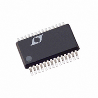
LTC3727EG-1#TR Linear Technology, LTC3727EG-1#TR Datasheet - Page 14

LTC3727EG-1#TR
Manufacturer Part Number
LTC3727EG-1#TR
Description
IC REG SW SYNC 2PH STPDWN 28SSOP
Manufacturer
Linear Technology
Series
PolyPhase®r
Type
Step-Down (Buck)r
Datasheet
1.LTC3727EGPBF.pdf
(32 pages)
Specifications of LTC3727EG-1#TR
Internal Switch(s)
No
Synchronous Rectifier
Yes
Number Of Outputs
2
Voltage - Output
0.8 ~ 14 V
Current - Output
25A
Frequency - Switching
250kHz ~ 550kHz
Voltage - Input
4 ~ 36 V
Operating Temperature
-40°C ~ 85°C
Mounting Type
Surface Mount
Package / Case
28-SSOP
Lead Free Status / RoHS Status
Contains lead / RoHS non-compliant
Power - Output
-
Available stocks
Company
Part Number
Manufacturer
Quantity
Price
APPLICATIO S I FOR ATIO
LTC3727/LTC3727-1
The inductor value also has secondary effects. The transi-
tion to Burst Mode operation begins when the average
inductor current required results in a peak current below
25% of the current limit determined by R
inductor values (higher ΔI
lower load currents, which can cause a dip in efficiency in
the upper range of low current operation. In Burst Mode
operation, lower inductance values will cause the burst
frequency to decrease.
Inductor Core Selection
Once the inductance value is determined, the type of
inductor must be selected. Actual core loss is independent
of core size for a fixed inductor value, but it is very
dependent on inductance selected. As inductance in-
creases, core losses go down. Unfortunately, increased
inductance requires more turns of wire and therefore
copper (I
Ferrite designs have very low core loss and are preferred
at high switching frequencies, so designers can concen-
trate on reducing I
Ferrite core material saturates “hard,” which means that
inductance collapses abruptly when the peak design cur-
rent is exceeded. This results in an abrupt increase in
inductor ripple current and consequent output voltage
ripple. Do not allow the core to saturate!
Different core materials and shapes will change the size/
current and price/current relationship of an inductor.
Toroid or shielded pot cores in ferrite or permalloy mate-
rials are small and don’t radiate much energy, but gener-
ally cost more than powdered iron core inductors with
similar characteristics. The choice of which style inductor
to use mainly depends on the price vs size requirements
and any radiated field/EMI requirements. New designs for
high current surface mount inductors are available from
numerous manufacturers, including Coiltronics, Vishay,
TDK, Pulse, Panasonic, Wuerth, Coilcraft, Toko and Sumida.
Power MOSFET and D1 Selection
Two external power MOSFETs must be selected for each
controller in the LTC3727: One N-channel MOSFET for the
top (main) switch, and one N-channel MOSFET for the
bottom (synchronous) switch.
14
2
R) losses will increase.
U
2
R loss and preventing saturation.
U
L
) will cause this to occur at
W
SENSE
U
. Lower
The peak-to-peak drive levels are set by the INTV
voltage. This voltage is typically 7.5V during start-up (see
EXTV
threshold MOSFETs must be used in most applications.
The only exception is if low input voltage is expected
(V
(V
BV
logic level MOSFETs are limited to 30V or less.
Selection criteria for the power MOSFETs include the “ON”
resistance R
input voltage and maximum output current. When the
LTC3727 is operating in continuous mode the duty cycles
for the top and bottom MOSFETs are given by:
The MOSFET power dissipations at maximum output
current are given by:
where δ is the temperature dependency of R
is a constant inversely related to the gate drive current.
Both MOSFETs have I
equation includes an additional term for transition losses,
which are highest at high input voltages. For V
high current efficiency generally improves with larger
MOSFETs, while for V
increase to the point that the use of a higher R
with lower C
synchronous MOSFET losses are greatest at high input
voltage when the top switch duty factor is low or during a
IN
GS(TH)
DSS
Main Switch Duty Cycle
P
P
Synchronous Switch Duty Cycle
MAIN
SYNC
< 5V); then, sub-logic level threshold MOSFETs
CC
specification for the MOSFETs as well; most of the
< 3V) should be used. Pay close attention to the
Pin Connection). Consequently, logic-level
=
=
k V
( ) (
V
V
RSS
DS(ON)
V
OUT
IN
IN
IN
–
V
2
actually provides higher efficiency. The
IN
(
V
I
I
MAX
MAX
, reverse transfer capacitance C
OUT
2
IN
R losses while the topside N-channel
)
)(
(
> 20V the transition losses rapidly
2
I
MAX
C
(
1 δ
RSS
+
=
)
2
V
)( )
)
V
(
OUT
R
1 δ
f
IN
DS ON
+
(
=
)
R
V
)
DS ON
IN
+
(
–
V
DS(ON)
IN
DS(ON)
V
)
IN
OUT
< 20V the
device
and k
RSS
3727fc
CC
,


