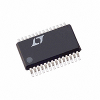
LTC3727EG-1#TR Linear Technology, LTC3727EG-1#TR Datasheet - Page 9

LTC3727EG-1#TR
Manufacturer Part Number
LTC3727EG-1#TR
Description
IC REG SW SYNC 2PH STPDWN 28SSOP
Manufacturer
Linear Technology
Series
PolyPhase®r
Type
Step-Down (Buck)r
Datasheet
1.LTC3727EGPBF.pdf
(32 pages)
Specifications of LTC3727EG-1#TR
Internal Switch(s)
No
Synchronous Rectifier
Yes
Number Of Outputs
2
Voltage - Output
0.8 ~ 14 V
Current - Output
25A
Frequency - Switching
250kHz ~ 550kHz
Voltage - Input
4 ~ 36 V
Operating Temperature
-40°C ~ 85°C
Mounting Type
Surface Mount
Package / Case
28-SSOP
Lead Free Status / RoHS Status
Contains lead / RoHS non-compliant
Power - Output
-
Available stocks
Company
Part Number
Manufacturer
Quantity
Price
FU CTIO AL DIAGRA
OPERATIO
Main Control Loop
The LTC3727/LTC3727-1 use a constant frequency, cur-
rent mode step-down architecture with the two controller
channels operating 180 degrees out of phase. During
normal operation, each top MOSFET is turned on when the
clock for that channel sets the RS latch, and turned off
when the main current comparator, I
The peak inductor current at which I
is controlled by the voltage on the I
output of each error amplifier EA. The V
R6
R5
V
F
IN
V
+
IN
R
7.5V
C
U
SEC
LP
LP
PLLFLTR
PGOOD
3.3V
EXTV
INTV
PLLIN
SGND
FCB
V
IN
OUT
50k
CC
0.18μA
CC
1.5V
U
OSCILLATOR
7.3V
PHASE DET
+
–
0.8V
U
7V
+
–
(Refer to Functional Diagram)
–
+
+
–
CLK1
CLK2
INTERNAL
–
–
–
–
+
+
+
+
SUPPLY
V
7.5V
LDO
REG
REF
0.86V
0.74V
0.86V
0.74V
BINH
FCB
V
V
OSENSE1
OSENSE2
W
1
1
DUPLICATE FOR SECOND
CONTROLLER CHANNEL
TH
, resets the RS latch.
resets the RS latch
OSENSE
pin, which is the
1.2μA
6V
pin receives
4(V
0.86V
FB
SLOPE
COMP
)
I1
S
R
+
–
0.55V
Q
Q
–
DROP
OUT
Figure 2
DET
25k
+
–
+
4(V
SHDN
+
RST
FB
B
3mV
)
the voltage feedback signal, which is compared to the
internal reference voltage by the EA. When the load current
increases, it causes a slight decrease in V
the 0.8V reference, which in turn causes the I
increase until the average inductor current matches the
new load current. After the top MOSFET has turned off, the
bottom MOSFET is turned on until either the inductor
current starts to reverse, as indicated by current compara-
tor I
BOT
TOP ON
–
SHDN
2
FCB
START
25k
SOFT
, or the beginning of the next cycle.
RUN
–
+
OV
2.4V
EA
I2
SWITCH
–
+
+
–
LOGIC
V
FB
0.80V
0.86V
TOP
BOT
INTV
LTC3727/LTC3727-1
CC
INTV
50k
50k
CC
V
SENSE
SENSE
RUN/SS
BOOST
PGND
OSENSE
SW
BG
I
TG
TH
+
–
INTV
CC
R1
C
D
C
C
B
D
R2
C2
SS
B
C
SEC
C
V
IN
R
C
D
R
OSENSE
1
SENSE
+
TH
C
C
voltage to
IN
SEC
relative to
3727fc
9


