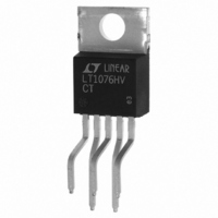
LT1076HVCT Linear Technology, LT1076HVCT Datasheet - Page 11

LT1076HVCT
Manufacturer Part Number
LT1076HVCT
Description
IC SWTCHNG REG STP-DWN 2A TO-220
Manufacturer
Linear Technology
Type
Step-Down (Buck), Step-Up (Boost), Inverting, Flybackr
Datasheet
1.LT1076CTPBF.pdf
(16 pages)
Specifications of LT1076HVCT
Internal Switch(s)
Yes
Synchronous Rectifier
No
Number Of Outputs
1
Voltage - Output
2.5 ~ 50 V
Current - Output
2A
Frequency - Switching
100kHz
Voltage - Input
8 ~ 64 V
Operating Temperature
0°C ~ 70°C
Mounting Type
Through Hole
Package / Case
TO-220-5 (Bent and Staggered Leads)
Lead Free Status / RoHS Status
Contains lead / RoHS non-compliant
Power - Output
-
Available stocks
Company
Part Number
Manufacturer
Quantity
Price
Company:
Part Number:
LT1076HVCT
Manufacturer:
LT
Quantity:
5 510
Part Number:
LT1076HVCT
Manufacturer:
LT/凌特
Quantity:
20 000
Part Number:
LT1076HVCT7-5#PBF
Manufacturer:
LINEAR/凌特
Quantity:
20 000
PI
I
The I
preset value of 6.5A. The equivalent circuit for this pin is
shown in Figure 8.
When I
through D2. Internal current limit is determined by the
current through Q1. If an external resistor is connected
between I
reduced for lower current limit. The resistor will have a
voltage across it equal to (320µA)(R), limited to ≈5V when
clamped by D2. Resistance required for a given current
limit is:
As an example, a 3A current limit would require
3A(2k) + 1k = 7kΩ for the LT1074. The accuracy of these
formulas is ±25% for 2A ≤ I
7A ≤ I
25% above the peak switch current required.
Foldback current limiting can be easily implemented by
adding a resistor from the output to the I
in Figure 9. This allows full desired current limit (with or
without R
current limit under short-circuit conditions. A typical value
for R
the amount of foldback. D2 prevents the output voltage
LIM
R
R
U
LIM
LIM
PIN
FB
LIM
LIM
DESCRIPTIO S
LIM
is 5kΩ, but this may be adjusted up or down to set
= I
= I
pin is used to reduce current limit below the
LIM
LIM
≤ 1.8A (LT1076), so I
is left open, the voltage at Q1 base clamps at 5V
LIM
LIM
) when the output is regulating, but reduces
and ground, the voltage at Q1 base can be
(2kΩ) + 1kΩ (LT1074)
(5.5kΩ) + 1kΩ (LT1076)
TO LIMIT
CIRCUIT
R1
8K
Q1
Figure 8. I
I
V
LIM
IN
D1
LIM
U
320 A
D2
Pin Circuit
µ
LIM
LIM
D3
6V
LT1047•PD12
should be set at least
≤ 5A (LT1074) and
4.3V
LIM
pin as shown
from forcing current back into the I
value for R
Example: I
Error Amplifier
The error amplifier in Figure 10 is a single stage design
with added inverters to allow the output to swing above
and below the common mode input voltage. One side of
the amplifier is tied to a trimmed internal reference voltage
of 2.21V. The other input is brought out as the FB (feed-
back) pin. This amplifier has a G
“out”) transfer function of ≈5000µmho. Voltage gain is
determined by multiplying G
output loading, consisting of the output resistance of Q4
and Q6 in parallel with the series RC external frequency
compensation network. At DC, the external RC is ignored,
and with a parallel output impedance for Q4 and Q6 of
400kΩ, voltage gain is ≈2000. At frequencies above a few
hertz, voltage gain is determined by the external compen-
sation, R
*Change 0.44 to 0.16, and 0.5 to 0.18 for LT1076.
R
R
FB
FB
=
=
C
0 5
(
0 5 9
1 5 0 44 9
and C
FB
LIM
. *
.
(
.
I
, first calculate R
SC
(
R
−
Figure 9. Foldback Current Limit
(
= 4A, ISC = 1.5A, R
LIM
R
k
−
C
L
−
I
.
.
LIM
0 44
− Ω
1
LT1074
.
k
1
)
)
R
k
( )
FB
−
*
k
)( )
1 5
)
Ω
FB
R
.
−
1N4148
L
LT1074/LT1076
D2
I
(
M
SC
3 8
LIM
.
times the total equivalent
M
(
R in k
k
, the R
(voltage “in” to current
LIM
Ω
L
LIM
)
LT1074•PD13
= (4)(2k) + 1k = 9k
pin. To calculate a
Ω
FB
V
OUT
:
)
sn1074 1074fds
11


