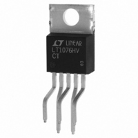
LT1076HVCT Linear Technology, LT1076HVCT Datasheet - Page 8

LT1076HVCT
Manufacturer Part Number
LT1076HVCT
Description
IC SWTCHNG REG STP-DWN 2A TO-220
Manufacturer
Linear Technology
Type
Step-Down (Buck), Step-Up (Boost), Inverting, Flybackr
Datasheet
1.LT1076CTPBF.pdf
(16 pages)
Specifications of LT1076HVCT
Internal Switch(s)
Yes
Synchronous Rectifier
No
Number Of Outputs
1
Voltage - Output
2.5 ~ 50 V
Current - Output
2A
Frequency - Switching
100kHz
Voltage - Input
8 ~ 64 V
Operating Temperature
0°C ~ 70°C
Mounting Type
Through Hole
Package / Case
TO-220-5 (Bent and Staggered Leads)
Lead Free Status / RoHS Status
Contains lead / RoHS non-compliant
Power - Output
-
Available stocks
Company
Part Number
Manufacturer
Quantity
Price
Company:
Part Number:
LT1076HVCT
Manufacturer:
LT
Quantity:
5 510
Part Number:
LT1076HVCT
Manufacturer:
LT/凌特
Quantity:
20 000
Part Number:
LT1076HVCT7-5#PBF
Manufacturer:
LINEAR/凌特
Quantity:
20 000
LT1074/LT1076
PI
V
The V
circuitry and one end of the high current switch. It is
important, especially at low input voltages , that this pin be
bypassed with a low ESR, and low inductance capacitor to
prevent transient steps or spikes from causing erratic
operation. At full switch current of 5A, the switching
transients at the regulator input can get very large as
shown in Figure 1. Place the input capacitor very close to
the regulator and connect it with wide traces to avoid extra
inductance. Use radial lead capacitors.
Input current on the V
of actual supply current (≈140µA, with a maximum of
300µA), and switch leakage current. Consult factory for
special testing if shutdown mode input current is critical.
GROUND PIN
It might seem unusual to describe a ground pin, but in the
case of regulators, the ground pin must be connected
properly to ensure good load regulation. The internal
reference voltage is referenced to the ground pin; so any
error in ground pin voltage will be multiplied at the output;
8
IN
L
“Spike” height (dI/dt • L
inch of lead length for LT1074 and 0.8V per inch for
LT1076.
“Step” for ESR = 0.05Ω and I
“Ramp” for C = 200µF, T
is 0.12V.
U
PIN
P
IN
= Total inductance in input bypass connections
DESCRIPTIO S
and capacitor.
pin is both the supply voltage for internal control
Figure 1. Input Capacitor Ripple
IN
Pin in shutdown mode is the sum
( )
( )
I
U
dt
P
dl
SW
STEP =
ON
) is approximately 2V per
( )
(
L
ESR
= 5µs, and I
P
SW
)
= 5A is 0.25V.
( )
SW
I
SW
RAMP =
C
= 5A,
(
LT1074•PD01
T
ON
)
To ensure good load regulation, the ground pin must be
connected directly to the proper output node, so that no
high currents flow in this path. The output divider resistor
should also be connected to this low current connection
line as shown in Figure 2.
FEEDBACK PIN
The feedback pin is the inverting input of an error amplifier
which controls the regulator output by adjusting duty
cycle. The noninverting input is internally connected to a
trimmed 2.21V reference. Input bias current is typically
0.5µA when the error amplifier is balanced (I
error amplifier has asymmetrical G
nals to reduce startup overshoot. This makes the amplifier
more sensitive to large ripple voltages at the feedback pin.
100mVp-p ripple at the feedback pin will create a 14mV
offset in the amplifier, equivalent to a 0.7% output voltage
shift. To avoid output errors, output ripple (P-P) should be
less than 4% of DC output voltage at the point where the
output divider is connected.
See the “Error Amplifier” section for more details.
Frequency Shifting at the Feedback Pin
The error amplifier feedback pin (FB) is used to downshift
the oscillator frequency when the regulator output voltage
is low. This is done to guarantee that output short-circuit
∆
V
OUT
HIGH CURRENT
RETURN PATH
=
Figure 2. Proper Ground Pin Connection
(
∆
LT1074
GND
V
GND
2 21
.
FB
)( )
V
OUT
NEGATIVE OUTPUT NODE
WHERE LOAD REGULATION
WILL BE MEASURED
R2
M
for large input sig-
LT1074•PD02
OUT
sn1074 1074fds
= 0). The


