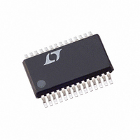
LTC1142HVCG#TRPBF Linear Technology, LTC1142HVCG#TRPBF Datasheet - Page 13

LTC1142HVCG#TRPBF
Manufacturer Part Number
LTC1142HVCG#TRPBF
Description
IC SW REG STEP-DOWN DUAL 28-SSOP
Manufacturer
Linear Technology
Type
Step-Down (Buck)r
Datasheet
1.LTC1142CG.pdf
(20 pages)
Specifications of LTC1142HVCG#TRPBF
Internal Switch(s)
No
Synchronous Rectifier
Yes
Number Of Outputs
2
Voltage - Output
3.3V, 5V
Current - Output
50mA
Frequency - Switching
250kHz
Voltage - Input
3.5 ~ 18 V
Operating Temperature
0°C ~ 70°C
Mounting Type
Surface Mount
Package / Case
28-SSOP
Lead Free Status / RoHS Status
Lead free / RoHS Compliant
Power - Output
-
Available stocks
Company
Part Number
Manufacturer
Quantity
Price
APPLICATIO S I FOR ATIO
current. When a load step occurs, V
amount equal to I
series resistance of C
or discharge C
current change and returns V
value. During this recovery time V
for overshoot or ringing which would indicate a stability
problem. The Pin 27 (13) external components shown in
the Figure 1 circuit will prove adequate compensation for
most applications.
A second, more severe transient is caused by switching in
loads with large (>1 F) supply bypass capacitors. The
discharged bypass capacitors are effectively put in parallel
with C
deliver enough current to prevent this problem if the load
switch resistance is low and it is driven quickly. The only
solution is to limit the rise time of the switch drive so that
the load rise time is limited to approximately 25 • C
Thus a 10 F capacitor would require a 250 s rise time,
limiting the charging current to about 200mA.
Efficiency Considerations
The percent efficiency of a switching regulator is equal to
the output power divided by the input power times 100%.
It is often useful to analyze individual losses to determine
what is limiting the efficiency and which change would
produce the most improvement. Percent efficiency can be
expressed as:
where L1, L2, etc., are the individual losses as a percent-
age of input power. (For high efficiency circuits only small
errors are incurred by expressing losses as a percentage
of output power.)
Although all dissipative elements in the circuit produce
losses, three main sources usually account for most of the
losses in LTC1142 circuits:
1. LTC1142 DC bias current
2. MOSFET gate charge current
3. I
1. The DC supply current is the current which flows into
%Efficiency = 100% – (L1 + L2 + L3 + ...)
V
2
IN
R losses
OUT
(pin 24 for the 3.3V section, Pin 10 for the 5V
, causing a rapid drop in V
OUT
LOAD
until the regulator loop adapts to the
U
OUT
• ESR, where ESR is the effective
. I
U
LOAD
OUT
also begins to charge
OUT
W
OUT
to its steady- state
can be monitored
. No regulator can
OUT
shifts by an
U
LOAD
.
2. MOSFET gate charge current results from switching
3. I
LTC1142/LTC1142L/LTC1142HV
section) less the gate charge current. For V
LTC1142 DC supply current for each section is 160 A
with no load, and increases proportionally with load up
to a constant 1.6mA after the LTC1142 has entered
continuous mode. Because the DC bias current is
drawn from V
voltage. For V
less than 1% for load currents over 30mA. However, at
very low load currents the DC bias current accounts for
nearly all of the loss.
the gate capacitance of the power MOSFETs. Each time
a MOSFET gate is switched from low to high to low
again, a packet of charge dQ moves from V
The resulting dQ/dt is a current out of V
typically much larger than the DC supply current. In
continuous mode, I
gate charge for a 0.1 N-channel power MOSFET is
25nC, and for a P-channel about twice that value. This
results in I
operation, for a 2% to 3% typical mid-current loss with
V
Note that the gate charge loss increases directly with
both input voltage and operating frequency. This is the
principal reason why the highest efficiency circuits
operate at moderate frequencies. Furthermore, it ar-
gues against using larger MOSFETs than necessary to
control I
well as money!
of the MOSFET, inductor, and current shunt. In continu-
ous mode the average output current flows through L
and R
and N-channel MOSFETs. If the two MOSFETs have
approximately the same R
one MOSFET can simply be summed with the resis-
tances of L and R
example, if each R
R
results in losses ranging from 3% to 12% as the output
current increases from 0.5A to 2A. I
efficiency to roll off at high output currents.
2
IN
SENSE
R losses are easily predicted from the DC resistances
= 10V.
SENSE
= 0.05 , then the total resistance is 0.3 . This
2
R losses, since overkill can cost efficiency as
GATE(CHG)
, but is “chopped” between the P-channel
IN
IN
, the resulting loss increases with input
= 10V the DC bias losses are generally
GATE(CHG)
DS(ON)
SENSE
= 7.5mA in 100kHz continuous
DS(ON)
to obtain I
= 0.1 , R
= f (Q
, then the resistance of
2
N
R losses cause the
+ Q
L
2
R losses. For
= 0.15 , and
P
). The typical
IN
IN
IN
to ground.
= 10V the
which is
13


