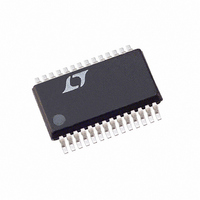
LTC1142HVCG#TRPBF Linear Technology, LTC1142HVCG#TRPBF Datasheet - Page 5

LTC1142HVCG#TRPBF
Manufacturer Part Number
LTC1142HVCG#TRPBF
Description
IC SW REG STEP-DOWN DUAL 28-SSOP
Manufacturer
Linear Technology
Type
Step-Down (Buck)r
Datasheet
1.LTC1142CG.pdf
(20 pages)
Specifications of LTC1142HVCG#TRPBF
Internal Switch(s)
No
Synchronous Rectifier
Yes
Number Of Outputs
2
Voltage - Output
3.3V, 5V
Current - Output
50mA
Frequency - Switching
250kHz
Voltage - Input
3.5 ~ 18 V
Operating Temperature
0°C ~ 70°C
Mounting Type
Surface Mount
Package / Case
28-SSOP
Lead Free Status / RoHS Status
Lead free / RoHS Compliant
Power - Output
-
Available stocks
Company
Part Number
Manufacturer
Quantity
Price
LTC1142/LTC1142HV
SENSE
Current Comparator. A built-in offset between Pins 1 and
28 in conjunction with R
threshold for the 3.3V section.
SHDN3 (Pin 2): When grounded, the 3.3V section oper-
ates normally. Pulling Pin 2 high holds both MOSFETs off
and puts the 3.3V section in micropower shutdown mode.
Requires CMOS logic-level signal with t
“float” Pin 2.
TYPICAL PERFOR A CE CHARACTERISTICS
PI FU CTIO S
2.1
1.8
1.5
1.2
0.9
0.6
0.3
28
24
20
16
12
U
8
4
0
0
20
DC Supply Current
0
Gate Charge Supply Current
+
PER REGULATOR BLOCK
NOT INCLUDING
GATE CHARGE CURRENT
PINS 10, 24
2
3 (Pin 1): The (+) Input to the 3.3V Section
OPERATING FREQUENCY (kHz)
U
80
4
Q
N
INPUT VOLTAGE (V)
+ Q
6
P
140
= 100nC
ACTIVE MODE
SLEEP MODE
8
Q
N
U
10
+ Q
200
P
12
= 50nC
SENSE3
W
14
260
1142 G10
16
1142 G07
U
18
sets the current trip
r
, t
f
80
70
60
50
40
30
20
10
20
18
16
14
12
10
< 1 s. Do not
0
8
6
4
2
0
0
Supply Current in Shutdown
Off-Time vs Output Voltage
0
PER REGULATOR BLOCK
PINS 10, 24
V
SHUTDOWN
2
V
OUT
1
4
OUTPUT VOLTAGE (V)
= 3.3V
INPUT VOLTAGE (V)
6
= 2V
2
8
SGND3 (Pin 3): The 3.3V section small-signal ground
must be routed separately from other grounds to the (–)
terminal of the 3.3V section output capacitor.
PGND3 (Pin 4): The 3.3V section driver power ground
connects to source of N-channel MOSFET and the (–)
terminal of the 3.3V section input capacitor.
NC (Pin 5): No Connection.
NDRIVE 3 (Pin 6): High Current Drive for Bottom N-Channel
MOSFET, 3.3V Section. Voltage swing at Pin 6 is from
ground to V
10
LTC1142/LTC1142L/LTC1142HV
V
3
OUT
V
12
SENSE
= 5V
14
4
= V
16
OUT
1142 G11
1142 G08
IN3
18
5
.
175
150
125
100
1.6
1.4
1.2
1.0
0.8
0.6
0.4
0.2
75
50
25
0
0
Operating Frequency vs
V
Current Sense Threshold Voltage
0
0
IN
V
OUT
– V
2
= 5V
20
OUT
V
IN
TEMPERATURE ( C)
4
– V
40
OUT
25 C
6
VOLTAGE (V)
0 C
60
THRESHOLD
THRESHOLD
MAXIMUM
MINIMUM
70 C
8
80
10
1142 G09
1142 G12
100
5
12


