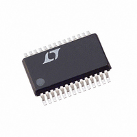
LTC1142HVCG#TRPBF Linear Technology, LTC1142HVCG#TRPBF Datasheet - Page 15

LTC1142HVCG#TRPBF
Manufacturer Part Number
LTC1142HVCG#TRPBF
Description
IC SW REG STEP-DOWN DUAL 28-SSOP
Manufacturer
Linear Technology
Type
Step-Down (Buck)r
Datasheet
1.LTC1142CG.pdf
(20 pages)
Specifications of LTC1142HVCG#TRPBF
Internal Switch(s)
No
Synchronous Rectifier
Yes
Number Of Outputs
2
Voltage - Output
3.3V, 5V
Current - Output
50mA
Frequency - Switching
250kHz
Voltage - Input
3.5 ~ 18 V
Operating Temperature
0°C ~ 70°C
Mounting Type
Surface Mount
Package / Case
28-SSOP
Lead Free Status / RoHS Status
Lead free / RoHS Compliant
Power - Output
-
Available stocks
Company
Part Number
Manufacturer
Quantity
Price
APPLICATIO S I FOR ATIO
To prevent stray pickup a 100pF capacitor is suggested
across R1 located close to the LTC1142HV-ADJ/LTC1142L-
ADJ as in Figure 6. The external divider network must be
placed across C
to signal ground. Refer to the Board Layout Checklist.
Board Layout Checklist
When laying out the printed circuit board, the following
checklist should be used to ensure proper operation of the
LTC1142. These items are also illustrated graphically in
V
V
OUT3
IN3
BOLD LINES INDICATE HIGH CURRENT PATHS
–
–
+
+
Figure 6. LTC1142-ADJ External Feedback Network
R
[PIN 2(16)]
[PIN 4(18)]
SENSE3
SGND
V
FB
OUT
C
with the negative plate of C
U
IN3
D1
+
100pF
L1
C
N-CH
OUT3
U
P-CH
R1
Figure 7. LTC1142 Layout Diagram (see Board Layout Checklist)
SHDN (3.3V OUTPUT)
C
T5
V
R2
IN5
W
1 F
1k
+
3300pF
+
R
SENSE
C
OUT
OUT
1142 F06
V
OUT
10
11
12
13
14
U
1
2
3
4
5
6
7
8
9
returned
NC
NC
PDRIVE 5
SENSE
SHDN3
SGND3
PGND3
NDRIVE 3
NC
V
C
INTV
I
SENSE
TH5
IN5
T5
CC5
–
+
3
5
1000pF
LTC1142
1000pF
NDRIVE 5
PDRIVE 3
the layout diagram of Figure 7. In general each block
should be self-contained with little cross coupling for best
performance. Check the following in your layout:
1. Are the signal and power grounds segregated? The
2. Does the LTC1142 Sense
3. Are the Sense
SENSE
SENSE
INTV
LTC1142/LTC1142L/LTC1142HV
PGND5
SGND5
SHDN5
LTC1142 signal ground [Pin 3 (17) for the LTC1142, Pin
4 (18) for LTC1142-ADJ] must return to the (–) plate of
C
N-channel MOSFET, anode of the Schottky diode,
and (–) plate of C
lengths as possible.
point close to R
minimum PC trace spacing? The 1000pF capacitor
between Pins 1 (15) and 28 (14) should be as close as
possible to the LTC1142. Ensure accurate current sens-
V
I
TH3
CC3
C
NC
IN3
NC
NC
OUT
–
+
T3
3
5
28
27
26
25
24
23
22
21
20
19
18
17
16
15
. The power ground returns to the source of the
SHDN (5V OUTPUT)
3300pF
+
1 F
V
–
IN3
and Sense
SENSE
IN
1k
, which should have as short lead
P-CH
and the (+) plate of C
C
T3
–
+
N-CH
C
, Pin 28 (14) connect to a
leads routed together with
OUT5
SENSE RESISTOR PCB PATTERN
+
D2
SENSE
L2
+
C
IN5
SENSE
R
SENSE5
–
OUT
15
–
+
–
+
V
1142 F07
V
?
OUT5
IN5


