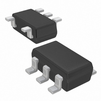
XC9133B02AMR-G Torex Semiconductor Ltd, XC9133B02AMR-G Datasheet

XC9133B02AMR-G
Specifications of XC9133B02AMR-G
Available stocks
Related parts for XC9133B02AMR-G
XC9133B02AMR-G Summary of contents
Page 1
XC9133 Series Step-Up DC/DC Converter-LED Backlight Driver ■GENERAL DESCRIPTION The XC9133 series is a fixed frequency, constant current step-up DC/DC converter which is optimized for LED backlight applications in mobile phones, PDAs and digital cameras. Output voltage ...
Page 2
XC9133 Series ■PIN CONFIGURATION SOT-25 (TOP VIEW) ■PIN ASSIGNMENT PIN NUMBER USP-6C SOT-25 (under development ■CE PIN FUNCTION CE PIN H L ■PRODUCT CLASSIFICATION ● Ordering Information (*1) ...
Page 3
DIAGRAMS ●XC9133B02A ■ ABSOLUTE MAXIMUM RATINGS PARAMETER V Pin Voltage IN Lx Pin Voltage FB Pin Voltage CE Pin Voltage Lx Pin Current SOT-25 Power Dissipation USP-6C (under development) Operating Temperature Range Storage Temperature Range SYMBOL RATINGS V V ...
Page 4
... XC9133 Series ■ELECTRICAL CHARACTERISTICS ●XC9133B02AMR PARAMETER SYMBOL FB Voltage V FB Output Voltage Range V OUTSET Input Voltage Range V IN Supply Current 1 I DD1 Supply Current 2 I DD2 Stand-by Current I STB Oscillation Frequency f OSC Maximum Duty Cycle MAXDTY (*1) Efficiency EFFI Current Limit I LIM Lx Overvoltage Limit ...
Page 5
APPLICATION CIRCUITS ●XC9133B02A ■EXTERNAL COMPONENTS SYMBOL VALUE L 22μH (*1) SBD - C 4.7μF IN (*3) C 0.22μF L NOTE: *1: Please use a Schottky barrier diode (SBD) with a low junction capacitance. *2: For using the XBS053V15R with ...
Page 6
XC9133 Series ■OPERATIONAL EXPLANATIONS (Continued) <Current Limit> The current limit circuit of the XC9133 series monitors the current flowing through the N-channel MOS driver transistor connected to the Lx pin, and features a combination of the constant-current type current limit ...
Page 7
INFORMATION <Dimming Control> 1. Applying PWM signal to the CE pin The XC9133 repeats on/off operations by a PWM signal applied to the CE pin. The magnitude of LED current, I when the diode is on, is determined by ...
Page 8
XC9133 Series ■APPLICATION INFORMATION (Continued) <Dimming Control (Continued)> 3. Using DC Voltage application it is necessary to control the LED current by a variable DC voltage, illumination control of LED is achieved by connecting R1 and R2 ...
Page 9
INFORMATION (Continued) <Illumination of Six in Total White LEDs> possible to illuminate three-series two parallel white LEDs, six in total, using an input voltage V Figure Circuit Illumination of Six in Total White LEDs <Use as Flash> ...
Page 10
XC9133 Series ■APPLICATION INFORMATION (Continued) <Separate Supply Source of the Step-up Circuit (V Supply source of the step-up circuit can be used separately from V Circuit example of separating supply source of the step-up circuit from V Note: Please input ...
Page 11
INFORMATION (Continued) <Instruction on Pattern Layout> order to stabilize V 's voltage level, we recommend that an input by-pass capacitor (C IN possible to the V & V pins Please mount each external component ...
Page 12
XC9133 Series ■TEST CIRCUITS ●Circuit ① (XC9133B02A Series) L:22uH CDRH3D16 XBS053V15R 4.7μF IN (ceramic ●Circuit ② ●Circuit ④ 1. The measurement method of L Using the circuit ④, ...
Page 13
INFORMATION ●SOT-25 (unit : mm) 2.9±0.2 +0.1 0.4 -0. +0.1 0.15 (0.95) -0.05 1.9±0.2 ●USP-6C (under development) 0~0.1 XC9133 Series * Pin no wider than other pins. 13/15 ...
Page 14
XC9133 Series ■ MARKING RULE ●SOT-25 ①Represents product series ② Represents Lx overvoltage limit SOT-25 (TOP VIEW) ③ Represents oscillation frequency ④ Represents production lot number and inverted characters and ...
Page 15
... Should you wish to use the products under conditions exceeding the specifications, please consult us or our representatives assume no responsibility for damage or loss due to abnormal use. 7. All rights reserved. No part of this datasheet may be copied or reproduced without the prior permission of TOREX SEMICONDUCTOR LTD. XC9133 Series 15/15 ...


