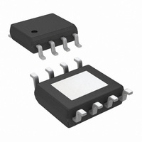
LM22673MRX-ADJ/NOPB National Semiconductor, LM22673MRX-ADJ/NOPB Datasheet - Page 9

LM22673MRX-ADJ/NOPB
Manufacturer Part Number
LM22673MRX-ADJ/NOPB
Description
IC REG SWITCH BUCK 3A ADJ 8PSOP
Manufacturer
National Semiconductor
Series
SIMPLE SWITCHER®r
Type
Step-Down (Buck)r
Datasheet
1.LM22673MRE-ADJNOPB.pdf
(18 pages)
Specifications of LM22673MRX-ADJ/NOPB
Internal Switch(s)
Yes
Synchronous Rectifier
No
Number Of Outputs
1
Voltage - Output
Adj to 1.285V
Current - Output
3A
Frequency - Switching
500kHz
Voltage - Input
4.5 ~ 42 V
Operating Temperature
-40°C ~ 125°C
Mounting Type
Surface Mount
Package / Case
8-PSOP
For Use With
551600236-001 - WEBENCH BUILD IT LM2267X 8-PSOPLM22673EVAL - BOARD EVALUATION FOR LM22673
Lead Free Status / RoHS Status
Lead free / RoHS Compliant
Power - Output
-
Other names
LM22673MRX-ADJ
Available stocks
Company
Part Number
Manufacturer
Quantity
Price
Company:
Part Number:
LM22673MRX-ADJ/NOPB
Manufacturer:
NS
Quantity:
59
The percentage of output current limit fold back is affected by
duty
See
The current limit will only protect the inductor from a runaway
condition if the LM22673 is operating in its safe operating
area. A runaway condition of the inductor is potentially catas-
trophic to the application. For every design, the safe operating
area needs to be calculated. Factors in determining the safe
operating area are the switching frequency, input voltage,
output voltage, minimum on-time and feedback voltage dur-
ing an over current condition.
As a first pass check, if the following equation holds true, a
given design is considered in a safe operating area and the
current limit will protect the circuit:
If the equation above does not hold true, the following sec-
ondary equation will need to hold true to be in safe operating
area:
If both equations do not hold true, a particular design will not
have an effective current limit function which might damage
the circuit during startup, over current conditions, or steady
state over current and short circuit condition. Oftentimes a
reduction of the maximum input voltage will bring a design into
the safe operating area.
Soft-Start
The soft-start feature allows the regulator to gradually reach
the initial steady state operating point, thus reducing start-up
stresses and surges. The soft-start can be adjusted by se-
lecting an external soft-start capacitor. An internal 50 µA
current source charges up the external soft-start capacitor.
The generated voltage is the voltage the internal reference
limits. If no external soft-start capacitor is used, there is an
internal soft-start feature with 500 µs (typical) start-up time.
Recommended soft-start capacitor values are between 100
nF to 1 µF.
Figure 3
cycle,
FIGURE 3. Output Current in Foldback vs.
for details.
V
inductance,
IN
x T
Nominal Duty Cycle
BLK
x F < V
and
OUT
switching
x 0.724
30076250
frequency.
9
Boot Pin
The LM22673 integrates an N-channel FET switch and as-
sociated floating high voltage level shift / gate driver. This gate
driver circuit works in conjunction with an internal diode and
an external bootstrap capacitor. A 0.01 µF ceramic capacitor
connected with short traces between the BOOT pin and the
SW pin is recommended to effectively drive the internal FET
switch. During the off-time of the switch, the SW voltage is
approximately -0.5V and the external bootstrap capacitor is
charged from the internal supply through the internal boot-
strap diode. When operating with a high PWM duty-cycle, the
buck switch will be forced off each cycle to ensure that the
bootstrap capacitor is recharged. See the maximum duty-cy-
cle section for more details.
Thermal Protection
Internal Thermal Shutdown circuitry protects the LM22673 in
the event the maximum junction temperature is exceeded.
When activated, typically at 150°C, the regulator is forced into
a low power reset state. There is a typical hysteresis of 15
degrees.
Internal Compensation
The LM22673 has an internal compensation designed for a
stable loop with a wide range of external power stage com-
ponents.
Insuring stability of a design with a specific power stage (in-
ductor and output capacitor) can be tricky. The LM22673
stability can be verified over varying loads and input and out-
put voltages using Webench
tion tool at www.national.com. A quick start spreadsheet can
also be downloaded from the online product folder.
The internal compensation of the -ADJ option of the LM22673
is optimized for output voltages below 5V. If an output voltage
of 5V or higher is needed, the -5.0 option with an additional
external resistor divider may also be used. The typical loca-
tion of the internal compensation poles and zeros as well as
the DC gain is given in
type III compensation allowing for the use of most output ca-
pacitors including ceramics.
This information can be used to calculate the transfer function
from the FB pin to the internal compensation node (input to
the PWM comparator in the block diagram).
For the power stage transfer function the standard voltage
mode formulas for the double pole and the ESR zero apply:
Corners
DC gain
Zero 1
Zero 2
Pole 1
Pole 2
Pole 3
Table
TABLE 1.
®
Designer online circuit simula-
1. The LM22673 has internal
Frequency
150 kHz
250 kHz
37.5 dB
1.5 kHz
100 Hz
15 kHz
www.national.com


