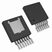
LM22673TJ-ADJ/NOPB National Semiconductor, LM22673TJ-ADJ/NOPB Datasheet - Page 8

LM22673TJ-ADJ/NOPB
Manufacturer Part Number
LM22673TJ-ADJ/NOPB
Description
IC REG SWITCH BUC 3A ADJ TO263-7
Manufacturer
National Semiconductor
Series
SIMPLE SWITCHER®r
Type
Step-Down (Buck)r
Datasheet
1.LM22673MRE-ADJNOPB.pdf
(18 pages)
Specifications of LM22673TJ-ADJ/NOPB
Internal Switch(s)
Yes
Synchronous Rectifier
No
Number Of Outputs
1
Voltage - Output
Adj to 1.285V
Current - Output
3A
Frequency - Switching
500kHz
Voltage - Input
4.5 ~ 42 V
Operating Temperature
-40°C ~ 125°C
Mounting Type
Surface Mount
Package / Case
TO-263-7 Thin
For Use With
551600233-001 - WEBENCH BUILD IT LM2267X TO-263LM22673EVAL - BOARD EVALUATION FOR LM22673
Lead Free Status / RoHS Status
Lead free / RoHS Compliant
Power - Output
-
Other names
LM22673TJ-ADJ
www.national.com
Detailed Operating Description
The LM22673 switching regulator features all of the functions
necessary to implement an efficient high voltage buck regu-
lator using a minimum of external components. This easy to
use regulator integrates a 42V N-Channel switch with an out-
put current capability of 3A. The regulator control method is
based on voltage mode control with input voltage feed for-
ward. The loop compensation is integrated into the LM22673
so that no external compensation components need to be se-
lected or utilized. Voltage mode control offers short minimum
on-times allowing short duty-cycles necessary in high input
voltage applications. The operating frequency is fixed at 500
kHz to allow for small external components while avoiding
excessive switching losses. The output voltage can be set as
low as 1.285V with the -ADJ device. Fault protection features
include current limiting and thermal shutdown. The device is
available in the TO-263 THIN and PSOP packages featuring
an exposed pad to aid thermal dissipation.
The functional block diagram with typical application of the
LM22673 is shown in
The internal compensation of the -ADJ option of the LM22673
is optimized for output voltages up to 5V. If an output voltage
of 5V or higher is needed, the -5.0 fixed output voltage option
with an additional external resistive feedback voltage divider
may also be used.
Maximum Duty-Cycle / Dropout
Voltage
The typical maximum duty-cycle is 90%. This corresponds to
a typical minimum off-time of 200 ns. This forced off-time is
important to provide enough time for the Cboot capacitor to
charge during each cycle. The lowest input voltage required
to maintain operation is:
Where V
Schottky diode and V
power N-FET of the LM22673. The R
specified in the electrical characteristics section of this
datasheet to calculate V
the switching frequency.
Minimum Duty-Cycle
Besides a minimum off-time, there is also a minimum on-time
which will take effect when the output voltage is adjusted very
low and the input voltage is very high. Should the operation
require an on-time shorter than minimum, individual switching
pulses will be skipped.
Pulse skipping is a normal mode of operation which appears
as a decrease in switching frequency. It has no effect on op-
eration or regulation except for an increase in output ripple
voltage. The pulse skipping function is required to maintain
proper regulation and overcurrent protection under the full
range of operating conditions.
The specified typical minimum on time of 100 ns is based on
the blanking time during current limit operation. During normal
operation, the minimum on-time will also include the effect of
propagation delay. Assume approximately 150 ns as a typical
operating minimum on time.
D
is the forward voltage drop across the re-circulating
Q
Figure
is the voltage drop across the internal
Q
according to the FET current. F is
1.
DS(ON)
of the FET is
8
where D is the duty-cycle.
Current Limit
When the power switch turns on, the slight capacitance load-
ing of the Schottky diode, D1, causes a leading-edge current
spike with an extended ringing period. This spike can cause
the current limit comparator to trip prematurely. A leading
edge blanking time (T
sampling the spike.
A key feature of the LM22673 is the ability to control the peak
switch current limit. Without this feature, the peak switch cur-
rent would be internally set to 4.2A (typical) to accommodate
3A load current designs. The high current limit requires that
both the inductor (which could saturate with excessively high
currents) and the catch diode be able to safely handle up to
4.2A under load fault condition.
If an application requires a load current less than 3A, the peak
switch current can be set to a limit just over the maximum load
current with the addition of a single programming resistor.
This allows the use of lower rated and more cost effective
inductors and diodes. A resistance of 10 kΩ sets the current
limit to typically 3.8A (typical) peak current and 20 kΩ reduces
the maximum peak current to 2A (typical).
When the switch current reaches the current limit threshold
the switch is immediately turned off. If T
minimum (100 ns typical) the switcher will hold the output
current flat at the set current limit value. But if T
decreases to the minimum T
frequency decreases to 1/5 the typical frequency. This effec-
tively causes the output current to fold back to a lower and
safe value. When the current limit condition is removed the
switching frequency is restored to nominal. This 5X frequency
fold back will result in a lower duty cycle pulse of the power
switch to minimize the overall fault condition power dissipa-
tion.
FIGURE 2. Peak Current Limit vs IADJ Resistor
BLK
) of 100 ns (typical) is used to avoid
ON
(100 ns typical) the switching
ON
is larger than the
30076213
ON
is at or


