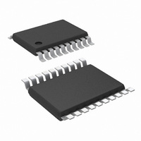
LM5005MH/NOPB National Semiconductor, LM5005MH/NOPB Datasheet - Page 15

LM5005MH/NOPB
Manufacturer Part Number
LM5005MH/NOPB
Description
IC BUCK SYNC ADJ 2.5A 20TSSOP
Manufacturer
National Semiconductor
Type
Step-Down (Buck)r
Datasheet
1.LM5005MHXNOPB.pdf
(22 pages)
Specifications of LM5005MH/NOPB
Internal Switch(s)
Yes
Synchronous Rectifier
No
Number Of Outputs
1
Voltage - Output
1.23 ~ 70 V
Current - Output
2.5A
Frequency - Switching
500kHz
Voltage - Input
7 ~ 75 V
Operating Temperature
-40°C ~ 125°C
Mounting Type
Surface Mount
Package / Case
20-TSSOP Exposed Pad, 20-eTSSOP, 20-HTSSOP
Power - Output
3.5W
Dc To Dc Converter Type
Inverting/Step Down
Pin Count
20
Input Voltage
75V
Output Voltage
1.225 to 70V
Switching Freq
50 TO 500KHz
Output Current
2.5A
Efficiency
90%
Package Type
TSSOP EP
Output Type
Adjustable
Switching Regulator
Yes
Mounting
Surface Mount
Input Voltage (min)
7V
Operating Temp Range
-40C to 125C
Operating Temperature Classification
Automotive
For Use With
LM5005EVAL - BOARD EVALUATION LM5005
Lead Free Status / RoHS Status
Lead free / RoHS Compliant
Other names
*LM5005MH
*LM5005MH/NOPB
LM5005MH
*LM5005MH/NOPB
LM5005MH
Available stocks
Company
Part Number
Manufacturer
Quantity
Price
Company:
Part Number:
LM5005MH/NOPB
Manufacturer:
TI
Quantity:
3 000
Part Number:
LM5005MH/NOPB
Manufacturer:
NS/国半
Quantity:
20 000
pacitance should be selected for RMS current rating and
minimum ripple voltage. A good approximation for the re-
quired ripple current rating necessary is I
Quality ceramic capacitors with a low ESR should be selected
for the input filter. To allow for capacitor tolerances and volt-
age effects, two 2.2 µF, 100V ceramic capacitors will be used.
If step input voltage transients are expected near the maxi-
mum rating of the LM5005, a careful evaluation of ringing and
possible spikes at the device VIN pin should be completed.
An additional damping network or input voltage clamp may be
required in these cases.
C8
The capacitor at the VCC pin provides noise filtering and sta-
bility for the V
should be no smaller than 0.1 µF, and should be a good qual-
ity, low ESR, ceramic capacitor. A value of 0.47 µF was
selected for this design.
C7
The bootstrap capacitor between the BST and the SW pins
supplies the gate current to charge the buck switch gate at
turn-on. The recommended value of C7 is 0.022 µF, and
should be a good quality, low ESR, ceramic capacitor.
C4
The capacitor at the SS pin determines the soft-start time, i.e.
the time for the reference voltage and the output voltage, to
reach the final regulated value. The time is determined from:
For this application, a C4 value of 0.01 µF was chosen which
corresponds to a soft-start time of 1 ms.
R5, R6
R5 and R6 set the output voltage level, the ratio of these re-
sistors is calculated from:
For a 5V output, the R5/R6 ratio calculates to 3.082. The re-
sistors should be chosen from standard value resistors, a
good starting point is selection in the range of 1.0 kΩ - 10
kΩ. Values of 5.11 kΩ for R5, and 1.65 kΩ for R6 were se-
lected.
R1, R2, C12
A voltage divider can be connected to the SD pin to set a
minimum operating voltage Vin
feature is required, the easiest approach to select the divider
resistor values is to select a value for R1 (between 10 kΩ and
100 kΩ recommended) then calculate R2 from:
Capacitor C12 provides filtering for the divider. The voltage at
the SD pin should never exceed 8V, when using an external
set-point divider it may be necessary to clamp the SD pin at
high input voltage conditions. The reference design utilizes
the full range of the LM5005 (7V to 75V); therefore these
CC
R5/R6 = (V
regulator. The recommended value of C8
OUT
/ 1.225V) - 1
(min)
for the regulator. If this
RMS
> I
OUT
/ 2.
15
components can be omitted. With the SD pin open circuit the
LM5005 responds once the Vcc UVLO threshold is satisfied.
R7, C11
A snubber network across the power diode reduces ringing
and spikes at the switching node. Excessive ringing and
spikes can cause erratic operation and couple spikes and
noise to the output. In the limit, spikes beyond the rating of
the LM5005 or the re-circulating diode can damage these de-
vices. Selecting the values for the snubber is best accom-
plished through empirical methods. First, make sure the lead
lengths for the snubber connections are very short. For the
current levels typical for the LM5005 a resistor value between
5 and 20 Ohms is adequate. Increasing the value of the snub-
ber capacitor results in more damping but higher losses.
Select a minimum value of C11 that provides adequate damp-
ing of the SW pin waveform at high load.
R4, C5, C6
These components configure the error amplifier gain charac-
teristics to accomplish a stable overall loop gain. One advan-
tage of current mode control is the ability to close the loop with
only two feedback components, R4 and C5. The overall loop
gain is the product of the modulator gain and the error ampli-
fier gain. The DC modulator gain of the LM5005 is as follows:
The dominant low frequency pole of the modulator is deter-
mined by the load resistance (R
(C
For R
DC Gain
For the design example of Figure 1 the following modulator
gain vs. frequency characteristic was measured as shown in
Figure 9.
OUT
LOAD
). The corner frequency of this pole is:
DC Gain
(MOD)
FIGURE 9. Gain and Phase of Modulator
= 5 Ω and C
R
LOAD
= 2 x 5 = 10 = 20 dB
f
(MOD)
p(MOD)
= 5 Ohms and C
= G
= 1 / (2π R
OUT
m(MOD)
= 177 µF then f
LOAD
x R
LOAD
,) and output capacitance
OUT
LOAD
C
= 177 µF
OUT
= 2 x R
p(MOD)
)
20161915
LOAD
www.national.com
= 180Hz


