LM2593HVS-5.0/NOPB National Semiconductor, LM2593HVS-5.0/NOPB Datasheet - Page 2
LM2593HVS-5.0/NOPB
Manufacturer Part Number
LM2593HVS-5.0/NOPB
Description
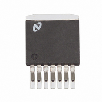
IC REG SW 5V 2A STP DN TO-263-7
Manufacturer
National Semiconductor
Series
SIMPLE SWITCHER®r
Type
Step-Down (Buck)r
Datasheet
1.LM2593HVS-ADJNOPB.pdf
(21 pages)
Specifications of LM2593HVS-5.0/NOPB
Internal Switch(s)
Yes
Synchronous Rectifier
No
Number Of Outputs
1
Voltage - Output
5V
Current - Output
2A
Frequency - Switching
150kHz
Voltage - Input
4.5 ~ 60 V
Operating Temperature
-40°C ~ 125°C
Mounting Type
Surface Mount
Package / Case
D²Pak, TO-263 (7 leads + tab)
Primary Input Voltage
12V
No. Of Outputs
1
Output Voltage
5V
Output Current
2A
No. Of Pins
7
Operating Temperature Range
-40°C To +125°C
Msl
MSL 3 - 168 Hours
Filter Terminals
SMD
Rohs Compliant
Yes
For Use With
LM2593HVEVAL - BOARD EVALUATION LM2593
Lead Free Status / RoHS Status
Lead free / RoHS Compliant
Power - Output
-
Other names
*LM2593HVS-5.0
*LM2593HVS-5.0/NOPB
LM2593HVS-5.0
*LM2593HVS-5.0/NOPB
LM2593HVS-5.0
Available stocks
Company
Part Number
Manufacturer
Quantity
Price

Part Number:
LM2593HVS-5.0/NOPB
Manufacturer:
NS/国半
Quantity:
20 000


www.national.com
SYSTEM PARAMETERS (Note 6) Test Circuit Figure 1
V
SYSTEM PARAMETERS (Note 6) Test Circuit Figure 1
V
SYSTEM PARAMETERS (Note 6) Test Circuit Figure 1
V
Symbol
Symbol
Symbol
FB
Absolute Maximum Ratings
If Military/Aerospace specified devices are required,
please contact the National Semiconductor Sales Office/
Distributors for availability and specifications.
LM2593HV-3.3
Electrical Characteristics
Specifications with standard type face are for T
ture Range.
OUT
LM2593HV-5.0
Electrical Characteristics
Specifications with standard type face are for T
ture Range.
OUT
LM2593HV-ADJ
Electrical Characteristics
Specifications with standard type face are for T
ture Range.
Maximum Supply Voltage (V
SD /SS Pin Input Voltage (Note 2)
Delay Pin Voltage (Note 2)
Flag Pin Voltage
Feedback Pin Voltage
Output Voltage to Ground
Power Dissipation
Storage Temperature Range
(Steady State)
Feedback Voltage
Output Voltage
Efficiency
Output Voltage
Efficiency
Parameter
Parameter
Parameter
IN
4.5V
V
)
OUT
4.75V
V
7V
V
IN
IN
programmed for 3V. Circuit of Figure 1 .
= 12V, I
V
= 12V, I
IN
V
IN
−65˚C to +150˚C
V
Internally limited
−0.3
IN
60V, 0.2A
−0.3
LOAD
60V, 0.2A
LOAD
J
J
J
60V, 0.2A
(Note 1)
= 25˚C, and those with boldface type apply over full Operating Tempera-
= 25˚C, and those with boldface type apply over full Operating Tempera-
= 25˚C, and those with boldface type apply over full Operating Tempera-
Conditions
V +25V
Conditions
Conditions
V 45V
= 2A
= 2A
1.5V
−1V
63V
6V
I
LOAD
I
LOAD
I
LOAD
2
2A
2A
Operating Conditions
ESD Susceptibility
Lead Temperature
Maximum Junction Temperature
Temperature Range
Supply Voltage
2A
Human Body Model (Note 3)
S Package
T Package (Soldering, 10 sec.)
Vapor Phase (60 sec.)
Infrared (10 sec.)
(Note 4)
(Note 4)
Typ
81
Typ
5
3.3
76
(Note 4)
1.230
LM2593HV-5.0
Typ
LM2593HV-3.3
LM2593HV-ADJ
4.800/4.750
5.200/5.250
3.168/3.135
3.432/3.465
(Note 5)
(Note 5)
1.193/1.180
1.267/1.280
Limit
Limit
(Note 5)
−40˚C
Limit
T
4.5V to 60V
J
(Limits)
(Limits)
+215˚C
+245˚C
+260˚C
+150˚C
+125˚C
V(max)
V(max)
V(min)
V(min)
Units
(Limits)
Units
V(max)
V(min)
Units
2 kV
%
V
V
V
Related parts for LM2593HVS-5.0/NOPB
Image
Part Number
Description
Manufacturer
Datasheet
Request
R

Part Number:
Description:
IC, STEP-DOWN REGULATOR, TO-263-7
Manufacturer:
National Semiconductor
Datasheet:
Part Number:
Description:
DC/DC Converter IC
Manufacturer:
National Semiconductor
Datasheet:

Part Number:
Description:
IC REG SW 3.3V 2A STP DN TO263-7
Manufacturer:
National Semiconductor
Datasheet:
Part Number:
Description:
IC REG SW ADJ 2A STP DN TO-263-7
Manufacturer:
National Semiconductor
Datasheet:

Part Number:
Description:
National Semiconductor [8-Bit D/A Converter]
Manufacturer:
National Semiconductor
Datasheet:
Part Number:
Description:
National Semiconductor [Media Coprocessor]
Manufacturer:
National Semiconductor
Datasheet:
Part Number:
Description:
Digitally Controlled Tone and Volume Circuit with Stereo Audio Power Amplifier, Microphone Preamp Stage and National 3D Sound
Manufacturer:
National Semiconductor
Datasheet:
Part Number:
Description:
Digitally Controlled Tone and Volume Circuit with Stereo Audio Power Amplifier, Microphone Preamp Stage and National 3D Sound
Manufacturer:
National Semiconductor
Datasheet:
Part Number:
Description:
AC97 Rev 2 Codec with Sample Rate Conversion and National 3D Sound
Manufacturer:
National Semiconductor
Part Number:
Description:
Manufacturer:
National Semiconductor
Datasheet:
Part Number:
Description:
Manufacturer:
National Semiconductor
Datasheet:
Part Number:
Description:
General Purpose, Low Voltage, Low Power, Rail-to-Rail Output Operational Amplifiers
Manufacturer:
National Semiconductor
Datasheet:
Part Number:
Description:
8-bit 20 MSPS flash A/D converter.
Manufacturer:
National Semiconductor
Datasheet: