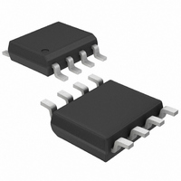
MAX1771CSA Maxim Integrated Products, MAX1771CSA Datasheet - Page 11

MAX1771CSA
Manufacturer Part Number
MAX1771CSA
Description
IC DC/DC CTRLR STEP-UP HE 8-SOIC
Manufacturer
Maxim Integrated Products
Type
Step-Up (Boost)r
Datasheet
1.MAX1771CPA.pdf
(16 pages)
Specifications of MAX1771CSA
Internal Switch(s)
No
Synchronous Rectifier
No
Number Of Outputs
1
Voltage - Output
12V, 2 ~ 16.5 V
Current - Output
2A
Frequency - Switching
300kHz
Voltage - Input
2 ~ 16.5 V
Operating Temperature
0°C ~ 70°C
Mounting Type
Surface Mount
Package / Case
8-SOIC (3.9mm Width)
Power - Output
471mW
Output Voltage
12 V
Output Current
2 A
Input Voltage
2 V to 16.5 V
Mounting Style
SMD/SMT
Maximum Operating Temperature
+ 70 C
Minimum Operating Temperature
0 C
Case
SOP8
Dc
02+
Lead Free Status / RoHS Status
Contains lead / RoHS non-compliant
Available stocks
Company
Part Number
Manufacturer
Quantity
Price
Company:
Part Number:
MAX1771CSA
Manufacturer:
MAX
Quantity:
7 031
Company:
Part Number:
MAX1771CSA
Manufacturer:
MAXIM
Quantity:
4
Part Number:
MAX1771CSA
Manufacturer:
MAXIM/美信
Quantity:
20 000
Company:
Part Number:
MAX1771CSA+T
Manufacturer:
NSC
Quantity:
6 219
Use an N-channel MOSFET power transistor with the
MAX1771.
To ensure the external N-channel MOSFET (N-FET) is
turned on hard, use logic-level or low-threshold
N-FETs when the input drive voltage is less than 8V. This
applies even in bootstrapped mode, to ensure start-up.
N-FETs provide the highest efficiency because they do
not draw any DC gate-drive current.
When selecting an N-FET, three important parameters
are the total gate charge (Q
and reverse transfer capacitance (C
Q
charging the gate. Use the typical Q
results; the maximum value is usually grossly over-
specified since it is a guaranteed limit and not the mea-
sured value. The typical total gate charge should be
50nC or less. With larger numbers, the EXT pins may
not be able to adequately drive the gate. The EXT
rise/fall time varies with different capacitive loads as
shown in the Typical Operating Characteristics.
The two most significant losses contributing to the
N-FET’s power dissipation are I
losses. Select a transistor with low r
C
Determine the maximum required gate-drive current
from the Q
The MAX1771’s maximum allowed switching frequency
during normal operation is 300kHz; but at start-up, the
maximum frequency can be 500kHz, so the maximum
current required to charge the N-FET’s gate is
f(max) x Q
transistor data sheet. For example, the Si9410DY has a
Q
required to charge the gate is:
The bypass capacitor on V+ (C2) must instantaneously
furnish the gate charge without excessive droop (e.g.,
less than 200mV):
Continuing with the example, ∆V+ = 17nC/0.1µF = 170mV.
Figure 2a’s application circuit uses an 8-pin Si9410DY
surface-mount N-FET that has 50mΩ on-resistance with
4.5V V
2b’s application circuit uses an MTD20N03HDL logic-
level N-FET with a guaranteed threshold voltage (V
of 2V.
RSS
g
g
(typ) of 17nC (at V
takes into account all capacitances associated with
to minimize these losses.
GS
I
GATE
, and a guaranteed V
g
g
(typ). Use the typical Q
specification in the N-FET data sheet.
(max) = (500kHz) (17nC) = 8.5mA.
______________________________________________________________________________________
Power Transistor Selection
∆V+ = ——
GS
= 5V), therefore the current
g
Q
C2
), on-resistance (r
TH
g
2
12V or Adjustable, High-Efficiency,
R losses and switching
of less than 3V. Figure
Low I
RSS
g
number from the
g
DS(ON)
).
value for best
and low
DS(ON)
Q
, Step-Up DC-DC Controller
TH
),
)
The MAX1771’s high switching frequency demands a
high-speed rectifier. Schottky diodes such as the
1N5817–1N5822 are recommended. Make sure the
Schottky diode’s average current rating exceeds the
peak current limit set by R
down voltage exceeds V
applications, Schottky diodes may be inadequate due
to their high leakage currents; high-speed silicon
diodes such as the MUR105 or EC11FS1 can be used
instead. At heavy loads and high temperatures, the
benefits of a Schottky diode’s low forward voltage may
outweigh the disadvantages of its high leakage current.
The primary criterion for selecting the output filter capac-
itor (C4) is low effective series resistance (ESR). The
product of the peak inductor current and the output filter
capacitor’s ESR determines the amplitude of the ripple
seen on the output voltage. Two OS-CON 150µF, 16V
output filter capacitors in parallel with 35mΩ of ESR each
typically provide 75mV ripple when stepping up from 5V
to 12V at 500mA (Figure 2a). Smaller-value and/or high-
er-ESR capacitors are acceptable for light loads or in
applications that can tolerate higher output ripple.
Since the output filter capacitor’s ESR affects efficien-
cy, use low-ESR capacitors for best performance. See
Table 1 for component selection.
The input bypass capacitor (C1) reduces peak currents
drawn from the voltage source and also reduces noise
at the voltage source caused by the switching action of
the MAX1771. The input voltage source impedance
determines the size of the capacitor required at the V+
input. As with the output filter capacitor, a low-ESR
capacitor is recommended. For output currents up to
1A, 68µF (C1) is adequate, although smaller bypass
capacitors may also be acceptable.
Bypass the IC with a 0.1µF ceramic capacitor (C2)
placed as close to the V+ and GND pins as possible.
Bypass REF with a 0.1µF capacitor (C3). REF can
source up to 100µA of current for external loads.
In adjustable output voltage and non-bootstrapped
modes, parallel a 47pF to 220pF capacitor across R2,
as shown in Figures 2 and 3. Choose the lowest capac-
itor value that insures stability; high capacitance values
may degrade line regulation.
OUT
SENSE
Input Bypass Capacitors
Capacitor Selection
Feed-Forward Capacitor
. For high-temperature
Output Filter Capacitor
Reference Capacitor
, and that its break-
Diode Selection
11


