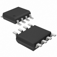
MAX1771CSA Maxim Integrated Products, MAX1771CSA Datasheet - Page 14

MAX1771CSA
Manufacturer Part Number
MAX1771CSA
Description
IC DC/DC CTRLR STEP-UP HE 8-SOIC
Manufacturer
Maxim Integrated Products
Type
Step-Up (Boost)r
Datasheet
1.MAX1771CPA.pdf
(16 pages)
Specifications of MAX1771CSA
Internal Switch(s)
No
Synchronous Rectifier
No
Number Of Outputs
1
Voltage - Output
12V, 2 ~ 16.5 V
Current - Output
2A
Frequency - Switching
300kHz
Voltage - Input
2 ~ 16.5 V
Operating Temperature
0°C ~ 70°C
Mounting Type
Surface Mount
Package / Case
8-SOIC (3.9mm Width)
Power - Output
471mW
Output Voltage
12 V
Output Current
2 A
Input Voltage
2 V to 16.5 V
Mounting Style
SMD/SMT
Maximum Operating Temperature
+ 70 C
Minimum Operating Temperature
0 C
Case
SOP8
Dc
02+
Lead Free Status / RoHS Status
Contains lead / RoHS non-compliant
Available stocks
Company
Part Number
Manufacturer
Quantity
Price
Company:
Part Number:
MAX1771CSA
Manufacturer:
MAX
Quantity:
7 031
Company:
Part Number:
MAX1771CSA
Manufacturer:
MAXIM
Quantity:
4
Part Number:
MAX1771CSA
Manufacturer:
MAXIM/美信
Quantity:
20 000
Company:
Part Number:
MAX1771CSA+T
Manufacturer:
NSC
Quantity:
6 219
carefully observe the component voltage ratings, since
some components must withstand the sum of the input
and output voltage (27V in this case). The circuit oper-
ates as an AC-coupled boost converter, and does not
change operating modes when crossing from buck to
boost. There is no instability around a 12V input.
Efficiency ranges from 85% at medium loads to about
82% at full load. Also, when shutdown is activated
(SHDN high) the output goes to 0V and sources no cur-
rent. A 1µF ceramic capacitor is used for C2. A larger
capacitor value improves efficiency by about 1% to 3%.
D2 ensures start-up for this AC-coupled configuration
by overriding the MAX1771’s Dual-Mode feature, which
allows the use of preset internal or user-set external
feedback. When operating in Dual-Mode, the IC first
12V or Adjustable, High-Efficiency,
Low I
Figure 6. 12V Buck/Boost from a 4.5V to 15V Input
14
OFF
0.1µF
ON
C5
NOTE: KEEP ALL TRACES CONNECTED
TO PIN 3 AS SHORT AS POSSIBLE
______________________________________________________________________________________
5
4
SHDN
REF
MAX1771
28kΩ
Q
1%
R3
4.5V TO 15V
V+
, Step-Up DC-DC Controller
2
V
IN
AGND
33µF
FB
GND
16V
EXT
C1
CS
3
D2*
1N4148
1
8
6
7
Q1**
L1
20µH
*SEE TEXT FOR FURTHER
**Q1 = MOTOROLA MMFT3055ELT1
1µF
R1
0.1Ω
C2*
COMPONENT INFORMATION
L1 + L2 = ONE COILTRONICS CTX20-4
200kΩ
1%
R2
1N5819
L2*
20µH
D1
NOTE: HIGH-
CURRENT GND
C3
100µF
16V
C4
100µF
16V
250mA
V
12V
OUT
tries to use internal feedback and looks to V+ for its
feedback signal. However, since V+ may be greater
than the internally set feedback (12V for the MAX1771),
the IC may think the output is sufficiently high and not
start. D2 ensures start-up by pulling FB above ground
and forcing the external feedback mode. In a normal
(not AC-coupled) boost circuit, D2 isn’t needed, since
the output and FB rise as soon as input power is
applied.
The circuit in Figure 7 uses a transformerless design to
supply 5V at 300mA from a -30V to -75V input supply.
The MAX1771 is biased such that its ground connec-
tions are made to the -48V input. The IC’s supply volt-
age (at V+) is set to about 9.4V (with respect to -48V)
by a zener-biased emitter follower (Q2). An N-channel
FET (Q1) is driven in a boost configuration. Output reg-
ulation is achieved by a transistor (Q3), which level
shifts a feedback signal from the 5V output to the IC’s
FB input. Conversion efficiency is typically 82%.
When selecting components, be sure that D1, Q1, Q2,
Q3, and C6 are rated for the full input voltage plus a
reasonable safety margin. Also, if D1 is substituted, it
should be a fast-recovery type with a t
R7, R9, C8, and D3 are optional and may be used to
soft start the circuit to prevent excessive current surges
at power-up.
The circuit in Figure 8 boosts two cells (2V min) to 24V
for LCD bias or other positive output applications.
Output power is boosted from the battery input, while
V+ voltage for the MAX1771 is supplied by a 5V or 3.3V
logic supply.
The circuit in Figure 9 boosts a 2.7V to 5.5V input to a
regulated 5V, 1A output for logic, RF power, or PCMCIA
applications. Efficiency vs. load current is shown in the
adjacent graph.
Transformerless -48V to +5V at 300mA
Battery-Powered LCD Bias Supply
5V, 1A Boost Converter
rr
less than 30ns.


