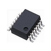
PC929PYJ000F Sharp Microelectronics, PC929PYJ000F Datasheet - Page 5

PC929PYJ000F
Manufacturer Part Number
PC929PYJ000F
Description
PHOTOCOUPLER OPIC 14-SMD
Manufacturer
Sharp Microelectronics
Series
OPIC™r
Datasheet
1.PC929J00000F.pdf
(22 pages)
Specifications of PC929PYJ000F
Voltage - Isolation
4000Vrms
Number Of Channels
1, Unidirectional
Current - Output / Channel
100mA
Propagation Delay High - Low @ If
300ns @ 5mA
Current - Dc Forward (if)
20mA
Input Type
DC
Output Type
Push-Pull, Totem-Pole
Mounting Type
Surface Mount
Package / Case
14-SMD
Configuration
1 Channel
Maximum Forward Diode Voltage
1.75 V
Maximum Reverse Diode Voltage
6 V
Maximum Power Dissipation
550 mW
Maximum Operating Temperature
+ 80 C
Minimum Operating Temperature
- 25 C
Isolation Voltage
5000 Vrms
Maximum Fall Time
0.2 us
Maximum Rise Time
0.5 us
Output Device
Integrated Photo IC
Lead Free Status / RoHS Status
Lead free / RoHS Compliant
*10 It shall connect a by-pass capacitor of 0.01 µF or more between V
*11 I
*12 V
overcurrent characteristics, Protection output characteristics, and Error signal output characteristics.
FLH
CTH
*11
*12
represents forward current when output goes from "Low" to "High"
is the of C(pin 9 ) voltage when output becomes from "High" to "Low"
Isolation resistance
Instantaneous common mode
rejection voltage
(High level output)
Instantaneous common mode
rejection voltage
(Low level output)
"Low→High" input threshold current
"Low→High" propagation delay time
"High→Low" propagation delay time
Rise time
Fall time
Overcurrent detection voltage
Overcurrent detection
voltage hysteresis width
O
time at overcurrent protection
O
O
at overcurrent protection
Low level error signal voltage
High level error signal voltage
Error signal "High→Low"
propagation delay time
Error signal output pulse width
2
2
2
"High→Low" propagation delay
Fall time at overcurrent protection
"High→Low" output voltage
Parameter
Symbol
t
t
V
CM
V
CM
PCOHL
t
V
R
PCFHL
V
∆t
I
t
t
I
PCOtf
PLH
PHL
FLH
FSH
CHIS
CTH
t
t
ISO
FSL
OE
r
f
CC
FS
H
L
(pin
13 )
T
T
V
a
a
=25˚C,V
and GND (pin
=25˚C, DC=500V, 40 to 60%RH
∆V
∆V
CC
T
T
=V
C
T
V
I
O2H
O2L
C
V
a
a
F
C
R
R
G
=25˚C, V
=25˚C, V
a
R
CC
=5mA, V
G
I
5
I
I
=25˚C, V
CC
=3 000pF, C
O1
G
V
G
F
F
C
G
FS
R
=2.0V, FS=OPEN, V
=2.0V, FS=OPEN, V
I
=3 000pF, FS=OPEN
C
T
CC
FS=OPEN, V
=0, V
=3 000pF, C=OPEN
=5mA, R
=47Ω, C
F
=V
=47Ω, C
=1kΩ, C
=V
FS
=24V, FS=OPEN, V
G
G
a
=10mA, R
=5mA, R
V
V
V
=V
=25˚C, I
=3 000pF, V
=47Ω, R
=24V, R
Conditions
CC
CC
CC
O1
FS=OPEN
T
O1
T
T
I
T
10
O1
F
a
=V
=V
=V
=24V, I
CC
a
a
a
=5mA,
=24V, I
=25˚C,
=24V, FS=OPEN, V
=25˚C
=25˚C
=25˚C
,
CM
CM
14
CC
=V
CC
O1
O1
O1
G
G
) near the device, when it measures the device, when it measures the
P
FS
=600V(p-p)
=600V(p-p)
=V
=3 000pF,
=V
=3 000pF
=3 000pF
F
=24V
G
=24V
=24V
C
O1
=5mA
G
=1.8kΩ
P
G
=47Ω
=1kΩ
=47Ω
=1 000pF
=47Ω
O1
=24V,
O1
F
C
F
=5mA,
=5mA
=0
*10
C
=24V,
=24V
=0
C
C
C
=0
=0
=0
C
=0
V
5×10
MIN.
(unless otherwise specified T
CC
−1.5
0.3
0.2
1.5
20
−
−
−
−
−
−
−
−
−
1
2
−6.5
PC929J00000F Series
10
V
TYP.
10
1.5
0.3
0.3
0.2
0.2
CC
0.2
35
−
−
−
−
−
2
4
5
1
11
−6
Sheet No.: D2-A06302EN
V
MAX.
CC
100
3.0
5.0
0.5
0.5
0.5
0.5
0.4
10
−
−
−
3
−
2
5
−
−5.5
kV/µs
kV/µs
Unit
mA
mA
a
µA
=T
µs
µs
µs
µs
µs
µs
µs
µs
Ω
V
V
V
V
opr
)


