M0216MD-162MDBR2-J Newhaven Display, M0216MD-162MDBR2-J Datasheet
M0216MD-162MDBR2-J
Specifications of M0216MD-162MDBR2-J


Related parts for M0216MD-162MDBR2-J


M0216MD-162MDBR2-J Summary of contents
Page 1
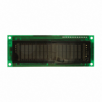
... M0216MD‐162MDBR2‐J Vacuum Fluorescent Display Module RoHS Compliant ...
Page 2
... Type Width Height Thickness [2] Changed by Table 1 M0216MD‐162MDBR2‐J 5x7 Dot with Cursor PT6314 Specifications 122.0 +‐ 1.0 44.0 +‐ 1.0 20.2 Max ...
Page 3
Parameter Display Size (W*H) Number of Digit Character Size (W*H) Character Pitch Dot Size Display Color 4.4 Environment Conditions Parameter Operating Temperature Storage Temperature Humidity (Operating) Humidity (Non‐operating) Vibration (10 ~ 55 Hz) Shock 4.5 Absolute Maximum Ratings Parameter Supply Voltage Input Signal Voltage 4.6 Recommend Operating Conditions Parameter Supply Voltage Signal (Logic) Input Voltage 4.7 DC Characteristics (Ta=+25°C, Vcc=+5.0Vdc) Parameter Supply Current High Level input current ...
Page 4
[4] ...
Page 5
Read/Write (R/W) control bit, the Register Select (RS) control bit, and a low bit. The following byte contains the instruction/data bits. The R/W bit determines whether the cycle is a read (high) or a write(low) cycle. The RS bit is used to identify the second byte as an instruction (low) or data(high).This mode uses the Strobe (STB) control signal, Serial Clock (SCK) input, and Serial I/O(SI/SO) line to transfer information. In a write cycle, bits are clocked into the module on the rising edge of SCK. In a read cycle, bits in the start byte are clocked into the module on the rising edge of SCK. After the minimum wait time, each bit in the instruction/data byte can be read from the module after each falling edge of SCK. Each read/write cycle begin son the falling edge of STB and ends on the rising edge. To be a valid read/write cycle, the STB must go high at the end of the cycle. [5] ...
Page 6
Fourteen (14) of through holes are prepared for power supply and data communications. A connector or pins may be able to soldered to the holes. [6] ...
Page 7
FUNCTION DESCRIPTIONS 1. 1.1 Registers in VFD Controller The VFD controller has two 8‐bit registers, an instruction register (IR) and a data register (DR). IR stores instruction codes, such as display clear and cursor shift, and address information for DD‐RAM and CG‐RAM. The IR can only be written from the host MPU. DR temporarily stores data to be written into DD‐RAM or CG‐RAM and temporarily stores data to be read from DD‐RAM or CG‐RAM by an internal operation. The DR is also used for data storage when reading data from DD‐RAM or CG‐RAM. When address information is written into the IR, data is read and then stored into the DR from DD‐RAM or CG‐RAM by internal operation. Data transfer between MPU is then completed when the MPU reads the DR. After the read, data in DD‐RAM or CG‐RAM at the next address is sent to the DFR for the next read from the MPU. By the register selector (RS) signal, these two registers can be selected (See Table 8). Fig 5 ...
Page 8
[8] ...
Page 9
[9] ...
Page 10
[10] ...
Page 11
[11] ...
Page 12
[12] ...
Page 13
[13] ...
Page 14
[14] ...
Page 15
[15] ...
Page 16
[16] ...
Page 17
[17] ...
Page 18
[18] ...