LMZ12003TZ-ADJ/NOPB National Semiconductor, LMZ12003TZ-ADJ/NOPB Datasheet - Page 9
LMZ12003TZ-ADJ/NOPB
Manufacturer Part Number
LMZ12003TZ-ADJ/NOPB
Description
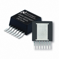
IC BUCK SYNC ADJ 3A TO-PMOD-7
Manufacturer
National Semiconductor
Series
SIMPLE SWITCHER®r
Type
Point of Load (POL) Non-Isolated with UVLOr
Datasheet
1.LMZ12003TZ-ADJNOPB.pdf
(16 pages)
Specifications of LMZ12003TZ-ADJ/NOPB
Output
0.8 ~ 6 V
Number Of Outputs
1
Power (watts)
18W
Mounting Type
Surface Mount
Voltage - Input
4.5 ~ 20V
Package / Case
TO-PMOD-7, Power Module
1st Output
0.8 ~ 6 VDC @ 3A
Size / Dimension
0.40" L x 0.54" W x 0.18" H (10.16mm x 13.77mm x 4.57mm)
Power (watts) - Rated
18W
Operating Temperature
-40°C ~ 125°C
Efficiency
92%
Approvals
EN
Operating Temperature (max)
125C
Operating Temperature (min)
-40C
Pin Count
7
Mounting
Surface Mount
Package Type
TO-PMOD EP
Case Length
10.16mm
Case Height
4.57mm
Screening Level
Automotive
Lead Free Status / RoHS Status
Lead free / RoHS Compliant
3rd Output
-
2nd Output
-
Lead Free Status / Rohs Status
Compliant
Other names
LMZ12003TZ-ADJTR
Available stocks
Company
Part Number
Manufacturer
Quantity
Price
Company:

Part Number:
LMZ12003TZ-ADJ/NOPB
Manufacturer:
NS
Quantity:
1 000


charging until it reaches approximately 3.8V on the SS pin.
Voltage levels between 0.8V and 3.8V have no effect on other
circuit operation. Note that the following conditions will reset
the soft-start capacitor by discharging the SS input to ground
with an internal 200 μA current sink.
• The enable input being “pulled low”
• Thermal shutdown condition
• Over-current fault
• Internal Vcc UVLO (Approx 4V input to V
C
None of the required C
in the module. At a minimum, the output capacitor must meet
the worst case minimum ripple current rating of 0.5 * I
as calculated in equation (19) below. Beyond that, additional
capacitance will reduce output ripple so long as the ESR is
low enough to permit it. A minimum value of 10 μF is generally
required. Experimentation will be required if attempting to op-
erate with a minimum value. Ceramic capacitors or other low
ESR types are recommended. See AN-2024 for more detail.
The following equation provides a good first pass approxima-
tion of C
C
Solving:
C
≥
The LMZ12003 demonstration and evaluation boards are
populated with a 100 uF 6.3V X5R output capacitor. Locations
for extra output capacitors are provided.
C
The LMZ12003 module contains an internal 0.47 µF input ce-
ramic capacitor. Additional input capacitance is required ex-
ternal to the module to handle the input ripple current of the
application. This input capacitance should be located in very
close proximity to the module. Input capacitor selection is
generally directed to satisfy the input ripple current require-
ments rather than by capacitance value. Worst case input
ripple current rating is dictated by the equation:
I(C
where D
(As a point of reference, the worst case ripple current will oc-
cur when the module is presented with full load current and
when V
Recommended minimum input capacitance is 10uF X7R ce-
ramic with a voltage rating at least 25% higher than the
maximum applied input voltage for the application. It is also
recommended that attention be paid to the voltage and tem-
perature deratings of the capacitor selected. It should be
noted that ripple current rating of ceramic capacitors may be
missing from the capacitor data sheet and you may have to
contact the capacitor manufacturer for this rating.
If the system design requires a certain minimum value of input
ripple voltage ΔV
may be used.
C
If ΔV
this equals 200 mV and f
C
≥
O
O
O
IN
IN
IN
52μF (7)
5.2μF
≥
≥
IN(RMS)
≥
SELECTION
SELECTION
≥
I
IN
STEP
3A*0.8V*6.8μH*12V / (4*3.3V*( 12V — 3.3V)*33mV)
3A * 3.3V/20V * (1– 3.3V/20V) / (400000 * 0.200 V)
I
O
is 1% of V
IN
O
* D * (1–D) / f
≊
)
*V
= 2 * V
for load transient requirements:
≊
V
FB
O
1 /2 * I
*L*V
/ V
O
IN
IN
IN
).
IN
be maintained then the following equation
O
for a 20V input to 3.3V output application
/ (4*V
*
SW-CCM
O
√
output capacitance is contained with-
SW
(D / 1-D) (8)
O
*(V
= 400 kHz.
* ΔV
IN
—V
IN
O
(9)
)*V
OUT-TRAN
IN
)
)(6)
LR P-P
,
9
Additional bulk capacitance with higher ESR may be required
to damp any resonant effects of the input capacitance and
parasitic inductance of the incoming supply lines.
R
Many designs will begin with a desired switching frequency in
mind. For that purpose the following equation can be used.
f
This can be rearranged as
R
The selection of RON and f
tations in the on-time and off-time for the COT control section.
The on-time of the LMZ12003 timer is determined by the re-
sistor R
t
The inverse relationship of t
switching frequency as VIN is varied. R
such that the on-time at maximum V
The on-timer has a limiter to ensure a minimum of 150 ns for
t
governed by the following equation:
f
This equation can be used to select R
frequency is desired so long as the minimum on-time of 150
ns is observed. The limit for R
R
If R
termined in (14) a lower frequency should be selected. Alter-
natively, V
frequency unchanged.
Additionally note, the minimum off-time of 260 ns limits the
maximum duty ratio. Larger R
lected in any application requiring large duty ratio.
Discontinuous Conduction and Continuous Conduction
Modes
At light load the regulator will operate in discontinuous con-
duction mode (DCM). With load currents above the critical
conduction point, it will operate in continuous conduction
mode (CCM). When operating in DCM the switching cycle
begins at zero amps inductor current; increases up to a peak
value, and then recedes back to zero before the end of the
off-time. Note that during the period of time that inductor cur-
rent is zero, all load current is supplied by the output capacitor.
The next on-time period starts when the voltage on the at the
FB pin falls below the internal reference. The switching fre-
quency is lower in DCM and varies more with load current as
compared to CCM. Conversion efficiency in DCM is main-
tained since conduction and switching losses are reduced
with the smaller load and lower switching frequency. Operat-
ing frequency in DCM can be calculated as follows:
f
In CCM, current flows through the inductor through the entire
switching cycle and never falls to zero during the off-time. The
switching frequency remains relatively constant with load cur-
rent and line voltage variations. The CCM operating frequen-
cy can be calculated using equation 7 above.
Following is a comparison pair of waveforms of the showing
both CCM (upper) and DCM operating modes.
SW(CCM)
ON
ON
SW(MAX)
SW(DCM)
ON
ON
ON
. This limits the maximum operating frequency, which is
= (1.3 * 10
ON
RESISTOR SELECTION
≊
≥
calculated in (11) is less than the minimum value de-
V
V
ON
≊
O
IN(MAX)
= V
≊
V
/ (1.3 * 10
and the input voltage V
V
IN(MAX)
O
O
O
*(V
/ (V
/ (1.3 * 10
-10
* 150 nsec / (1.3 * 10
IN
* R
-1)*6.8μH*1.18*10
IN(MAX)
can also be limited in order to keep the
ON
-10
) / V
* f
-10
* 150 nsec) (13)
SW(CCM)
IN
* R
ON
SW(CCM)
(12)
ON
and V
ON
ON
can be calculated as follows:
) (10)
IN
(lower F
(11)
. It is calculated as follows:
must be confined by limi-
20
IN
IN
ON
-10
*I
gives a nearly constant
is greater than 150 ns.
ON
O
) (14)
if a certain operating
/(V
should be selected
SW
IN
) should be se-
–V
O
www.national.com
)*R
ON
2
(15)
Related parts for LMZ12003TZ-ADJ/NOPB
Image
Part Number
Description
Manufacturer
Datasheet
Request
R

Part Number:
Description:
3A SIMPLE SWITCHER� Power Module with 20V Maximum
Manufacturer:
NSC [National Semiconductor]
Datasheet:

Part Number:
Description:
IC BUCK SYNC ADJ 3A TO-PMOD-7
Manufacturer:
National Semiconductor
Datasheet:

Part Number:
Description:
National Semiconductor [8-Bit D/A Converter]
Manufacturer:
National Semiconductor
Datasheet:
Part Number:
Description:
National Semiconductor [Media Coprocessor]
Manufacturer:
National Semiconductor
Datasheet:
Part Number:
Description:
Digitally Controlled Tone and Volume Circuit with Stereo Audio Power Amplifier, Microphone Preamp Stage and National 3D Sound
Manufacturer:
National Semiconductor
Datasheet:
Part Number:
Description:
Digitally Controlled Tone and Volume Circuit with Stereo Audio Power Amplifier, Microphone Preamp Stage and National 3D Sound
Manufacturer:
National Semiconductor
Datasheet:
Part Number:
Description:
AC97 Rev 2 Codec with Sample Rate Conversion and National 3D Sound
Manufacturer:
National Semiconductor
Part Number:
Description:
Manufacturer:
National Semiconductor
Datasheet:
Part Number:
Description:
Manufacturer:
National Semiconductor
Datasheet:
Part Number:
Description:
General Purpose, Low Voltage, Low Power, Rail-to-Rail Output Operational Amplifiers
Manufacturer:
National Semiconductor
Datasheet:
Part Number:
Description:
8-bit 20 MSPS flash A/D converter.
Manufacturer:
National Semiconductor
Datasheet:
Part Number:
Description:
Low Noise Quad Operational Amplifier
Manufacturer:
National Semiconductor
Datasheet:
Part Number:
Description:
Quad Differential Line Receivers
Manufacturer:
National Semiconductor
Datasheet:
Part Number:
Description:
Quad High Speed Trapezoidal? Bus Transceiver
Manufacturer:
National Semiconductor
Datasheet: