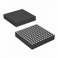
LTM4615EV#PBF Linear Technology, LTM4615EV#PBF Datasheet - Page 14

LTM4615EV#PBF
Manufacturer Part Number
LTM4615EV#PBF
Description
IC SWIT REG BUCK 4A ADJ 144LGA
Manufacturer
Linear Technology
Series
µModuler
Type
Point of Load (POL) Non-Isolatedr
Specifications of LTM4615EV#PBF
Design Resources
LTM4615 Spice Model
Output
0.8 ~ 5 V
Number Of Outputs
3
Power (watts)
12W
Mounting Type
Surface Mount
Voltage - Input
2.38 ~ 5.5 V
Package / Case
144-LGA
1st Output
0.8 ~ 5 VDC @ 4A
2nd Output
0.8 ~ 5 VDC @ 4A
3rd Output
0.8 ~ 5 VDC @ 4A
Size / Dimension
0.59" L x 0.59" W x 0.11" H (15mm x 15mm x 2.8mm)
Power (watts) - Rated
12W
Operating Temperature
-40°C ~ 125°C
Efficiency
95%
Primary Input Voltage
5.5V
No. Of Outputs
3
Output Voltage
5V
Output Current
1.5A
Voltage Regulator Case Style
LGA
No. Of Pins
144
Operating Temperature Range
-40°C To +125°C
Rohs Compliant
Yes
Lead Free Status / RoHS Status
Lead free / RoHS Compliant
Available stocks
Company
Part Number
Manufacturer
Quantity
Price
LTM4615
APPLICATIONS INFORMATION
VLDO SECTION
Adjustable Output Voltage
The output voltage is set by the ratio of two resistors. A
4.99k resistor is built onboard the module from LDO_OUT
to FB3. An additional resistor (R
to GND3 to set the output voltage over a range of 0.4V to
2.6V. Minimum output current of 1mA is required for full
output voltage range.
The equation:
Power Good Operation
The VLDO includes an open-drain power good (PGOOD3)
pin with hysteresis. If the VLDO is in shutdown or under
UVLO conditions (BOOST3 < 4.2V), then PGOOD3 is low
impedance to ground. PGOOD3 becomes high imped-
ance when the VLDO output voltage rises to 93% of its
regulated voltage. PGOOD3 stays high impedance until
the output voltage falls to 91% of its regulated voltage. A
pull-up resistor can be inserted between the PGOOD3 pin
and a positive logic supply such as the VLDO output or
V
good to operate properly.
Output Capacitance and Transient Response
The VLDO is designed to be stable with a wide range of
ceramic output capacitors. The ESR of the output capaci-
tors affects stability, especially smaller value capacitors. An
output capacitor of 10μF or greater with an ESR of 0.05Ω
or less is recommended to ensure stability. Larger value
capacitors can be used to reduce the transient deviations
under load changes. Bypass capacitors that are used at
the load device can also increase the effective output
capacitance. High ESR tantalum or electrolytic bulk ca-
pacitance can be used, but a ceramic capacitor must be
used in parallel at the output.
Extra consideration should be given to the use of ceramic
capacitors related to dielectrics, temperature and DC bias
effects on the capacitor. The VLDO requires a minimum
14
IN
V
. LDO_IN should be at least 1.14V or greater for power
OUT
=
0 4
.
V
•
4 99
.
R
k R
FBLDO
+
FBLDO
FBLDO
)is required from FB3
10μF value. The X7R and X5R dielectrics are more stable
with DC bias and temperature, thus more preferred.
Short-Circuit/Thermal Protection
The VLDO has built-in short-circuit current limiting of
~3A as well as overtemperature protection. During short-
circuit conditions the device is in control to 3A, and as
the internal temperature rises to approximately 150°C,
then the internal boost and LDO are shut down until the
internal temperature drops back to 140°C. The device will
cycle in and out of this mode with no latchup or damage.
Long term over stress in this condition can degrade the
device over time.
Reverse Current Protection
The VLDO features reverse current protection to limit
current draw from any supplementary power source at
the output. Figure 4 shows the reverse output current
limit for constant input and output cases. Note: Positive
input current represents current fl owing into the LDO_IN
pin. With LDO_OUT held at or below the output regula-
tion voltage and LDO_IN varied, input current fl ow will
follow Figure 4 curves. Input reverse current ramps up
to 16μA as the LDO_IN approaches LDO_OUT. Reverse
input current will spike up as LDO_IN approaches with in
30mV of LDO_OUT as reverse current protection circuitry
is disabled and normal operation resumes. As LDO_IN
transitions above LDO_OUT the reverse current transi-
tions into short circuit current as long as LDO_OUT is
held below the regulation voltage.
Figure 4. Reverse Current Limit for VLDO
–10
–20
–30
30
20
10
0
0
0.3
INPUT VOLTAGE (V)
0.6
LIMIT ABOVE 1.45V
IN CURRENT
0.9
1.2
1.5
4615 F04
1.8
4615f


