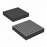
LTM4615EV#PBF Linear Technology, LTM4615EV#PBF Datasheet - Page 18

LTM4615EV#PBF
Manufacturer Part Number
LTM4615EV#PBF
Description
IC SWIT REG BUCK 4A ADJ 144LGA
Manufacturer
Linear Technology
Series
µModuler
Type
Point of Load (POL) Non-Isolatedr
Specifications of LTM4615EV#PBF
Design Resources
LTM4615 Spice Model
Output
0.8 ~ 5 V
Number Of Outputs
3
Power (watts)
12W
Mounting Type
Surface Mount
Voltage - Input
2.38 ~ 5.5 V
Package / Case
144-LGA
1st Output
0.8 ~ 5 VDC @ 4A
2nd Output
0.8 ~ 5 VDC @ 4A
3rd Output
0.8 ~ 5 VDC @ 4A
Size / Dimension
0.59" L x 0.59" W x 0.11" H (15mm x 15mm x 2.8mm)
Power (watts) - Rated
12W
Operating Temperature
-40°C ~ 125°C
Efficiency
95%
Primary Input Voltage
5.5V
No. Of Outputs
3
Output Voltage
5V
Output Current
1.5A
Voltage Regulator Case Style
LGA
No. Of Pins
144
Operating Temperature Range
-40°C To +125°C
Rohs Compliant
Yes
Lead Free Status / RoHS Status
Lead free / RoHS Compliant
Available stocks
Company
Part Number
Manufacturer
Quantity
Price
LTM4615
APPLICATIONS INFORMATION
Safety Considerations
The LTM4615 modules do not provide isolation from V
V
with a rating twice the maximum input current needs to be
provided to protect each unit from catastrophic failure.
Layout Checklist/Example
The high integration of LTM4615 makes the PCB board
layout very simple and easy. However, to optimize its electri-
cal and thermal performance, some layout considerations
are still necessary.
• Use large PCB copper areas for high current path,
18
OUT
including V
PCB conduction loss and thermal stress.
. There is no internal fuse. If required, a slow blow fuse
IN
, GND and V
CONTROL
SW1
OUT
LD0_IN
GND1
GND1
GND3
GND2
GND2
V
V
IN1
IN2
. It helps to minimize the
C
IN2
C
C
IN3
IN1
M
L
K
H
G
D
J
F
E
C
B
A
1
Figure 11. Recommended PCB Layout
2
3
GND1 CONTROL
GND2
4
IN
5
SW2
to
6
7
• Place high frequency ceramic input and output capaci-
• Place a dedicated power ground layer underneath the
• To minimize the via conduction loss and reduce module
• Do not put via directly on pads unless the via is
Figure 11 gives a good example of the recommended
layout.
8
tors next to the V
high frequency noise.
unit.
thermal stress, use multiple vias for interconnection
between the top layer and other power layers.
capped.
9
10 11 12
GND2
V
OUT1
C
C
OUT1
OUT4
C
OUT3
IN
C
C
OUT2
OUT5
, GND and V
4615 F11
V
GND1
LDO_OUT
GND3
V
GND2
OUT1
OUT2
OUT
pins to minimize
4615f


