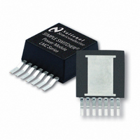
LMZ10504TZX-ADJ/NOPB National Semiconductor, LMZ10504TZX-ADJ/NOPB Datasheet

LMZ10504TZX-ADJ/NOPB
Specifications of LMZ10504TZX-ADJ/NOPB
Related parts for LMZ10504TZX-ADJ/NOPB
LMZ10504TZX-ADJ/NOPB Summary of contents
Page 1
... Refer to JA Board Application Note: AN-2022. Note 2: EN 55022:2006, +A1:2007, FCC Part 15 Subpart B: 2007. See Figure 5 and layout for information on device under test. © 2010 National Semiconductor Corporation LMZ10504 Performance Benefits ■ Operates at high ambient temperatures ■ ...
Page 2
... Connection Diagram Ordering Information Order Number Supplied As LMZ10504TZE-ADJ 45 Units in a Rail LMZ10504TZ-ADJ 250 Units in Tape and Reel LMZ10504TZX-ADJ 500 Units in Tape and Reel Pin Descriptions Pin Number Name 1 VIN Power supply input. A low ESR input capacitance should be located as close as possible to the VIN pin and exposed pad (EP) ...
Page 3
... Absolute Maximum Ratings If Military/Aerospace specified devices are required, please contact the National Semiconductor Sales Office/ Distributors for availability and specifications. VIN, VOUT, EN, FB GND ESD Susceptibility (Note 4) Power Dissipation Junction Temperature Electrical Characteristics apply over the operating junction temperature range T test, design, or statistical correlation. Typical values represent the most likely parametric norm at T reference purposes only ...
Page 4
Electrical Characteristics apply over the operating junction temperature range T test, design, or statistical correlation. Typical values represent the most likely parametric norm at T reference purposes only Symbol Parameter PERFORMANCE PARAMETERS ΔV Output Voltage ...
Page 5
Typical Performance Characteristics V = 5.0V µF 10V X5R ceramic capacitor Load Transient Response V = 3.3V 2.5V 0.4A to 3.6A to 0.4A step IN OUT OUT 20 mV/DIV, 20 ...
Page 6
Efficiency V = 3.3V OUT Efficiency V = 1.8V OUT Efficiency V = 1.2V OUT www.national.com 30088271 30088269 30088268 6 Efficiency V = 2.5V OUT 30088270 Efficiency V = 1.5V OUT 300882a0 Efficiency V = 0.8V OUT 30088267 ...
Page 7
Current Derating = 5V, θ 20° Radiated Emissions (EN 55022, Class 5V 2.5V OUT OUT Evaluation Board Pre-biased Startup V = 2.5V ...
Page 8
Block Diagram General Description The LMZ10504 SIMPLE SWITCHER® power module is a complete, easy-to-use DC-DC solution capable of driving load with exceptional power conversion efficiency, output voltage accuracy, line and load regulation. The LMZ10504 is available ...
Page 9
A second criteria before finalizing the C the RMS current capability. The necessary RMS current rat- ing of the input capacitor to a buck regulator can be estimated by With this high AC current present in the input capacitor, the ...
Page 10
C (µF) Voltage (V), R (mΩ) O ESR 22 6.3, < 6.3, < 6.3, < 10.0, < 5 100 6.3, < 5 100 6.3, 50 100 6.3, 25 150 6.3, 18 330 6.3, 18 ...
Page 11
Estimate Power Dissipation And Board Thermal Requirements Use the current derating curves in the typical performance characteristics section to obtain an estimate of power loss (P ). For the design case of V IC_LOSS 4A ...
Page 12
ADDITIONAL FEATURES Enable The LMZ10504 features an enable (EN) pin and associated comparator to allow the user to easily sequence the LMZ10504 from an external voltage rail manually set the input UVLO threshold. The turn-on or rising threshold ...
Page 13
For example, if the master supply voltage V the LMZ10504 output voltage was 1.8V, then the value of R needed to give the two ...
Page 14
LMZ10504 Application Circuit Schematic and BOMs This section provides several application solutions with an associated bill of materials. The compensation for each solu- tion was optimized to work over the full input range. Many TABLE 3. Bill of Materials, V ...
Page 15
TABLE 5. Bill of Materials 3. Designator Description U1 SIMPLE SWITCHER® µF, X5R, 10V in1 C 220 µF, 10V, AL-Elec in2 C 4.7 µF, X5R, 10V µF, X5R, 6.3V ...
Page 16
TABLE 7. Bill of Materials, V Designator Description U1 SIMPLE SWITCHER® µF, X7R, 16V in1 4.7 µF, X5R, 6.3V in2 µF, X5R, 16V in3 µF, X5R, 6.3V ...
Page 17
TABLE 9. Bill of Materials 5V Designator Description U1 SIMPLE SWITCHER® µF, X7R, 16V in1 C 4.7 µF, X5R, 6.3V in2 C 47 µF, X5R, 6.3V in3 C 100 µF, X5R, 6. ...
Page 18
PCB Layout Diagrams The PCB design is available in the LMZ10504 product folder at www.national.com. www.national.com FIGURE 6. Top Copper FIGURE 7. Internal Layer 1 (Ground) 18 30088276 30088277 ...
Page 19
FIGURE 8. Internal Layer 2 (Ground and Signal Traces) FIGURE 9. Bottom Copper 19 30088278 30088279 www.national.com ...
Page 20
Physical Dimensions www.national.com inches (millimeters) unless otherwise noted TO-PMOD-7 Pin Package NS Package Number TZA07A 20 ...
Page 21
21 www.national.com ...
Page 22
... For more National Semiconductor product information and proven design tools, visit the following Web sites at: www.national.com Products Amplifiers www.national.com/amplifiers Audio www.national.com/audio Clock and Timing www.national.com/timing Data Converters www.national.com/adc Interface www.national.com/interface LVDS www.national.com/lvds Power Management www.national.com/power Switching Regulators www.national.com/switchers LDOs www.national.com/ldo LED Lighting www ...


