LMZ14202TZE-ADJ/NOPB National Semiconductor, LMZ14202TZE-ADJ/NOPB Datasheet - Page 14
LMZ14202TZE-ADJ/NOPB
Manufacturer Part Number
LMZ14202TZE-ADJ/NOPB
Description
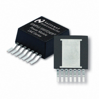
IC BUCK SYNC ADJ 2A TO-PMOD-7
Manufacturer
National Semiconductor
Series
SIMPLE SWITCHER®r
Type
Point of Load (POL) Non-Isolated with UVLOr
Datasheet
1.LMZ14202TZ-ADJNOPB.pdf
(18 pages)
Specifications of LMZ14202TZE-ADJ/NOPB
Output
0.8 ~ 6 V
Number Of Outputs
1
Power (watts)
12W
Mounting Type
Surface Mount
Voltage - Input
6 ~ 42 V
Package / Case
TO-PMOD-7, Power Module
1st Output
0.8 ~ 6 VDC @ 2A
Size / Dimension
0.40" L x 0.54" W x 0.18" H (10.16mm x 13.77mm x 4.57mm)
Power (watts) - Rated
12W
Operating Temperature
-40°C ~ 125°C
Efficiency
90%
Approvals
EN
Lead Free Status / RoHS Status
Lead free / RoHS Compliant
3rd Output
-
2nd Output
-
Available stocks
Company
Part Number
Manufacturer
Quantity
Price
Company:

Part Number:
LMZ14202TZE-ADJ/NOPB
Manufacturer:
TI
Quantity:
15 600


www.national.com
Additional Features
OUTPUT OVER-VOLTAGE COMPARATOR
The voltage at FB is compared to a 0.92V internal reference.
If FB rises above 0.92V the on-time is immediately terminat-
ed. This condition is known as over-voltage protection (OVP).
It can occur if the input voltage is increased very suddenly or
if the output load is decreased very suddenly. Once OVP is
activated, the top MOSFET on-times will be inhibited until the
condition clears. Additionally, the synchronous MOSFET will
remain on until inductor current falls to zero.
CURRENT LIMIT
Current limit detection is carried out during the off-time by
monitoring the current in the synchronous MOSFET. Refer-
ring to the Functional Block Diagram, when the top MOSFET
is turned off, the inductor current flows through the load, the
PGND pin and the internal synchronous MOSFET. If this cur-
rent exceeds 2.6 A (typical) the current limit comparator dis-
ables the start of the next on-time period. The next switching
cycle will occur only if the FB input is less than 0.8V and the
inductor current has decreased below 2.6 A. Inductor current
is monitored during the period of time the synchronous MOS-
FET is conducting. So long as inductor current exceeds 2.6A,
further on-time intervals for the top MOSFET will not occur.
Switching frequency is lower during current limit due to the
longer off-time. It should also be noted that current limit is
dependent on both duty cycle and temperature as illustrated
in the graphs in the typical performance section.
THERMAL PROTECTION
The junction temperature of the LMZ14202 should not be al-
lowed to exceed its maximum ratings. Thermal protection is
implemented by an internal Thermal Shutdown circuit which
activates at 165 °C (typ) causing the device to enter a low
power standby state. In this state the main MOSFET remains
off causing V
discharged to ground. Thermal protection helps prevent
catastrophic failures for accidental device overheating. When
the junction temperature falls back below 145 °C (typ Hyst =
20 °C) the SS pin is released, V
operation resumes.
Applications requiring maximum output current especially
those at high input voltage may require application derating
at elevated temperatures.
ZERO COIL CURRENT DETECTION
The current of the lower (synchronous) MOSFET is monitored
by a zero coil current detection circuit which inhibits the syn-
chronous MOSFET when its current reaches zero until the
next on-time. This circuit enables the DCM operating mode,
which improves efficiency at light loads.
O
to fall, and additionally the CSS capacitor is
O
rises smoothly, and normal
14
PRE-BIASED STARTUP
The LMZ14202 will properly start up into a pre-biased output.
This startup situation is common in multiple rail logic applica-
tions where current paths may exist between different power
rails during the startup sequence. The following scope cap-
ture shows proper behavior during this event.
Pre-Biased Startup
30114525
Related parts for LMZ14202TZE-ADJ/NOPB
Image
Part Number
Description
Manufacturer
Datasheet
Request
R

Part Number:
Description:
National Semiconductor [8-Bit D/A Converter]
Manufacturer:
National Semiconductor
Datasheet:
Part Number:
Description:
National Semiconductor [Media Coprocessor]
Manufacturer:
National Semiconductor
Datasheet:
Part Number:
Description:
Digitally Controlled Tone and Volume Circuit with Stereo Audio Power Amplifier, Microphone Preamp Stage and National 3D Sound
Manufacturer:
National Semiconductor
Datasheet:
Part Number:
Description:
Digitally Controlled Tone and Volume Circuit with Stereo Audio Power Amplifier, Microphone Preamp Stage and National 3D Sound
Manufacturer:
National Semiconductor
Datasheet:
Part Number:
Description:
AC97 Rev 2 Codec with Sample Rate Conversion and National 3D Sound
Manufacturer:
National Semiconductor
Part Number:
Description:
Manufacturer:
National Semiconductor
Datasheet:
Part Number:
Description:
Manufacturer:
National Semiconductor
Datasheet:
Part Number:
Description:
General Purpose, Low Voltage, Low Power, Rail-to-Rail Output Operational Amplifiers
Manufacturer:
National Semiconductor
Datasheet:
Part Number:
Description:
8-bit 20 MSPS flash A/D converter.
Manufacturer:
National Semiconductor
Datasheet:
Part Number:
Description:
Low Noise Quad Operational Amplifier
Manufacturer:
National Semiconductor
Datasheet:
Part Number:
Description:
Quad Differential Line Receivers
Manufacturer:
National Semiconductor
Datasheet:
Part Number:
Description:
Quad High Speed Trapezoidal? Bus Transceiver
Manufacturer:
National Semiconductor
Datasheet:
Part Number:
Description:
Dual Line Receiver
Manufacturer:
National Semiconductor
Datasheet:
Part Number:
Description:
TTL to 10k ECL Level Translator with Latch
Manufacturer:
National Semiconductor
Datasheet: