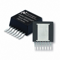
LMZ14203TZX-ADJ/NOPB National Semiconductor, LMZ14203TZX-ADJ/NOPB Datasheet

LMZ14203TZX-ADJ/NOPB
Specifications of LMZ14203TZX-ADJ/NOPB
Related parts for LMZ14203TZX-ADJ/NOPB
LMZ14203TZX-ADJ/NOPB Summary of contents
Page 1
... Point of load conversions from 12V and 24V input rail ■ Time critical projects ■ Space constrained / high thermal requirement applications ■ Negative output voltage applications (See AN-2027) © 2010 National Semiconductor Corporation LMZ14203 Performance Benefits ■ Operates at high ambient temperature with no thermal derating ■ ...
Page 2
... Simplified Application Schematic Connection Diagram Ordering Information Order Number LMZ14203TZ-ADJ LMZ14203TZX-ADJ LMZ14203TZE-ADJ Pin Descriptions Pin Name Description 1 VIN Supply input — Nominal operating range 42V . A small amount of internal capacitance is contained within the package assembly. Additional external input capacitance is required between this pin and exposed pad. ...
Page 3
Pin Name Description 6 FB Feedback — Internally connected to the regulation, over-voltage, and short-circuit comparators. The regulation reference point is 0.8V at this input pin. Connected the feedback resistor divider between the output and ground to set the output ...
Page 4
... Absolute Maximum Ratings If Military/Aerospace specified devices are required, please contact the National Semiconductor Sales Office/ Distributors for availability and specifications. VIN, RON to GND EN, FB GND Junction Temperature Storage Temperature Range Electrical Characteristics junction temperature (T ) range of -40°C to +125°C. Minimum and Maximum limits are guaranteed through test, design or statistical J correlation ...
Page 5
Symbol Parameter η Efficiency η Efficiency Note 1: Absolute Maximum Ratings are limits beyond which damage to the device may occur. Operating Ratings are conditions under which operation of the device is intended to be functional. For guaranteed specifications and ...
Page 6
Efficiency 24V Input @ 25°C Efficiency 36V Input @ 25°C Efficiency 6V Input @ 85°C www.national.com Dissipation 24V Input @ 25°C 30107026 Dissipation 36V Input @ 25°C 30107029 Dissipation 6V input @ 85°C 30107033 6 30107027 30107030 30107034 ...
Page 7
Efficiency 8V input 85°C 30107040 Efficiency 12V input@ 85°C 30107042 Efficiency 24V input @ 85°C 30107044 Dissipation 8V input 85°C Dissipation 12V input @ 85°C Dissipation 24V input @ 85°C 7 30107041 30107043 30107045 www.national.com ...
Page 8
Efficiency 36V input @ 85°C Line and Load Regulation @ 25°C Transient Response 24V 3.3V 0. Step IN O www.national.com Dissipation 36V input @ 85°C 30107046 24V IN 30107048 Thermal Derating V 30107006 8 30107047 Output Ripple 3.3V ...
Page 9
Application Block Diagram COT Control Circuit Overview Constant On Time control is based on a comparator and an on-time one shot, with the output voltage feedback compared with an internal 0.8V reference. If the feedback voltage is be- low the ...
Page 10
These resistors should be chosen from values in the range of 1.0 kohm to 10.0 kohm. For V = 0.8V the FB pin can be connected to the output di- O rectly so long as an output preload resistor remains ...
Page 11
V can also be limited in order to keep the IN(MAX) frequency unchanged. Additionally note, the minimum off-time of 260 ns limits the maximum duty ratio. Larger R (lower F ON lected in any application requiring large duty ratio. ...
Page 12
Good layout can be imple- mented by following a few simple design rules. 1. Minimize area of switched current loops. From an EMI reduction standpoint imperative to minimize the high di/dt paths during ...
Page 13
PRE-BIASED STARTUP The LMZ14203 will properly start up into a pre-biased output. This startup situation is common in multiple rail logic applica- tions where current paths may exist between different power rails during the startup sequence. The following scope cap- ...
Page 14
... ENT R 11.8 kΩ ENB C 22 nF, ±10%, X7R, 16V nF, ±10%, X7R, 16V SS www.national.com Case Size Case Size TO-PMOD-7 National Semiconductor 1206 Taiyo Yuden 1210 Taiyo Yuden 1206 Taiyo Yuden 1210 Taiyo Yuden 0603 Vishay Dale 0603 Vishay Dale 0603 Vishay Dale ...
Page 15
15 30107016 30107017 www.national.com ...
Page 16
Physical Dimensions www.national.com inches (millimeters) unless otherwise noted 7-Lead TZA Package NS Package Number TZA07A 16 ...
Page 17
Notes 17 www.national.com ...
Page 18
... For more National Semiconductor product information and proven design tools, visit the following Web sites at: www.national.com Products Amplifiers www.national.com/amplifiers Audio www.national.com/audio Clock and Timing www.national.com/timing Data Converters www.national.com/adc Interface www.national.com/interface LVDS www.national.com/lvds Power Management www.national.com/power Switching Regulators www.national.com/switchers LDOs www.national.com/ldo LED Lighting www ...


