AC164112 Microchip Technology, AC164112 Datasheet - Page 65
AC164112
Manufacturer Part Number
AC164112
Description
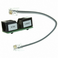
VOLTAGE LIMITER MPLAB ICD2 VPP
Manufacturer
Microchip Technology
Datasheet
1.AC164112.pdf
(302 pages)
Specifications of AC164112
Accessory Type
Voltage Limiter
Product
Cable Assemblies
Features
Programming And Debugging The Latest PIC12/PIC16/PIC18 Products
Development Tool Type
Hardware - Eval/Demo Board
Lead Free Status / RoHS Status
Lead free / RoHS Compliant
For Use With/related Products
MPLAB®
Lead Free Status / Rohs Status
Lead free / RoHS Compliant
For Use With
MPLAB ICD 2
Lead Free Status / RoHS Status
Lead free / RoHS Compliant, Lead free / RoHS Compliant
Available stocks
Company
Part Number
Manufacturer
Quantity
Price
Company:

Part Number:
AC164112
Manufacturer:
Microchip Technology
Quantity:
135


6.3.4
Each PORTB pin is multiplexed with other functions. The
pins and their combined functions are briefly described
here. For specific information about individual functions
such as the SSP, I
section in this data sheet.
6.3.4.1
Figure 6-7 shows the diagram for this pin. This pin is
configurable to function as one of the following:
• a general purpose I/O
• an analog input for the ADC
• a capacitive sensing input
• an external edge triggered interrupt
6.3.4.2
Figure 6-8 shows the diagram for this pin. This pin is
configurable to function as one of the following:
• a general purpose I/O
• an analog input for the ADC
• a capacitive sensing input
6.3.4.3
Figure 6-8 shows the diagram for this pin. This pin is
configurable to function as one of the following:
• a general purpose I/O
• an analog input for the ADC
• a capacitive sensing input
6.3.4.4
Figure 6-9 shows the diagram for this pin. This pin is
configurable to function as one of the following:
• a general purpose I/O
• an analog input for the ADC
• a capacitive sensing input
• a Capture 2 input, Compare 2 output, and PWM2
6.3.4.5
Figure 6-8 shows the diagram for this pin. This pin is
configurable to function as one of the following:
• a general purpose I/O
• an analog input for the ADC
• a capacitive sensing input
© 2009 Microchip Technology Inc.
output
Note:
PIN DESCRIPTIONS AND
DIAGRAMS
CCP2 pin location may be selected as
RB3 or RC1.
RB0/AN12/CPS0/INT
RB1/AN10/CPS1
RB2/AN8/CPS2
RB3/AN9/CPS3/CCP2
RB4/AN11/CPS4
2
C or interrupts, refer to the appropriate
PIC16F72X/PIC16LF72X
6.3.4.6
Figure 6-10 shows the diagram for this pin. This pin is
configurable to function as one of the following:
• a general purpose I/O
• an analog input for the ADC
• a capacitive sensing input
• a Timer1 gate input
6.3.4.7
Figure 6-11 shows the diagram for this pin. This pin is
configurable to function as one of the following:
• a general purpose I/O
• In-Circuit Serial Programming clock
6.3.4.8
Figure 6-12 shows the diagram for this pin. This pin is
configurable to function as one of the following:
• a general purpose I/O
• In-Circuit Serial Programming data
RB5/AN13/CPS5/T1G
RB6/ICSPCLK
RB7/ICSPDAT
DS41341E-page 65
Related parts for AC164112
Image
Part Number
Description
Manufacturer
Datasheet
Request
R

Part Number:
Description:
Manufacturer:
Microchip Technology Inc.
Datasheet:
Part Number:
Description:
Manufacturer:
Microchip Technology Inc.
Datasheet:
Part Number:
Description:
Manufacturer:
Microchip Technology Inc.
Datasheet:
Part Number:
Description:
Manufacturer:
Microchip Technology Inc.
Datasheet:
Part Number:
Description:
Manufacturer:
Microchip Technology Inc.
Datasheet:
Part Number:
Description:
Manufacturer:
Microchip Technology Inc.
Datasheet:
Part Number:
Description:
Manufacturer:
Microchip Technology Inc.
Datasheet:
Part Number:
Description:
Manufacturer:
Microchip Technology Inc.
Datasheet: