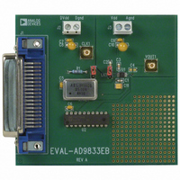
EVAL-AD9833EBZ Analog Devices Inc, EVAL-AD9833EBZ Datasheet - Page 12
EVAL-AD9833EBZ
Manufacturer Part Number
EVAL-AD9833EBZ
Description
BOARD EVAL FOR AD9833
Manufacturer
Analog Devices Inc
Datasheet
1.AD9833BRMZ.pdf
(24 pages)
Specifications of EVAL-AD9833EBZ
Main Purpose
Timing, Direct Digital Synthesis (DDS)
Embedded
No
Utilized Ic / Part
AD9833
Primary Attributes
10-Bit DAC, 28-Bit Tuning Word Width
Secondary Attributes
25MHz, Graphical User Interface, 2.3 V ~ 5.5 V
Lead Free Status / RoHS Status
Lead free / RoHS Compliant
Other names
EVAL-AD9833EB
EVAL-AD9833EB
EVAL-AD9833EB
Available stocks
Company
Part Number
Manufacturer
Quantity
Price
Company:

Part Number:
EVAL-AD9833EBZ
Manufacturer:
Analog Devices Inc
Quantity:
135


AD9833
CIRCUIT DESCRIPTION
The AD9833 is a fully integrated direct digital synthesis (DDS)
chip. The chip requires one reference clock, one low precision
resistor, and decoupling capacitors to provide digitally created
sine waves up to 12.5 MHz. In addition to the generation of this
RF signal, the chip is fully capable of a broad range of simple
and complex modulation schemes. These modulation schemes
are fully implemented in the digital domain, allowing accurate
and simple realization of complex modulation algorithms using
DSP techniques.
The internal circuitry of the AD9833 consists of the following
main sections: a NCO, frequency and phase modulators, SIN
ROM, a DAC, and a regulator.
NUMERICALLY CONTROLLED OSCILLATOR PLUS
PHASE MODULATOR
This consists of two frequency select registers, a phase accumulator,
two phase offset registers, and a phase offset adder. The main
component of the NCO is a 28-bit phase accumulator. Continuous
time signals have a phase range of 0 to 2π. Outside this range of
numbers, the sinusoid functions repeat themselves in a periodic
manner. The digital implementation is no different. The
accumulator simply scales the range of phase numbers into a
multibit digital word. The phase accumulator in the AD9833 is
implemented with 28 bits. Therefore, in the AD9833, 2π = 228.
Likewise, the ΔPhase term is scaled into this range of numbers
0 < ΔPhase < 2
becomes
where 0 < ΔPhase < 2
The input to the phase accumulator can be selected either from
the FREQ0 register or FREQ1 register and is controlled by the
FSELECT bit. NCOs inherently generate continuous phase
signals, thus avoiding any output discontinuity when switching
between frequencies.
Following the NCO, a phase offset can be added to perform
phase modulation using the 12-bit phase registers. The contents
of one of these phase registers are added to the most significant
bits of the NCO. The AD9833 has two phase registers; their
resolution is 2π/4096.
f = ΔPhase × f
28
− 1. With these substitutions, the previous equation
MCLK
28
∕2
− 1
28
Rev. C | Page 12 of 24
SIN ROM
To make the output from the NCO useful, it must be converted
from phase information into a sinusoidal value. Because phase
information maps directly into amplitude, the SIN ROM uses the
digital phase information as an address to a look-up table and
converts the phase information into amplitude. Although the NCO
contains a 28-bit phase accumulator, the output of the NCO is
truncated to 12 bits. Using the full resolution of the phase
accumulator is impractical and unnecessary, because this would
require a look-up table of 2
sufficient phase resolution such that the errors due to truncation
are smaller than the resolution of the 10-bit DAC. This requires
that the SIN ROM have two bits of phase resolution more than
the 10-bit DAC.
The SIN ROM is enabled using the mode bit (D1) in the control
register. This is explained further in Table 15.
DIGITAL-TO-ANALOG CONVERTER (DAC)
The AD9833 includes a high impedance, current source 10-bit
DAC. The DAC receives the digital words from the SIN ROM
and converts them into the corresponding analog voltages.
The DAC is configured for single-ended operation. An external
load resistor is not required because the device has a 200 Ω
resistor on board. The DAC generates an output voltage of
typically 0.6 V p-p.
REGULATOR
VDD provides the power supply required for the analog section
and the digital section of the AD9833. This supply can have a
value of 2.3 V to 5.5 V.
The internal digital section of the AD9833 is operated at 2.5 V.
An on-board regulator steps down the voltage applied at VDD
to 2.5 V. When the applied voltage at the VDD pin of the AD9833
is equal to or less than 2.7 V, the CAP/2.5 V and VDD pins
should be tied together, thus bypassing the on-board regulator.
28
entries. It is necessary only to have
Related parts for EVAL-AD9833EBZ
Image
Part Number
Description
Manufacturer
Datasheet
Request
R


Part Number:
Description:
BOARD EVAL FOR SI270X-A
Manufacturer:
Silicon Laboratories Inc
Datasheet:

Part Number:
Description:
BUCK CONV REF DESIGN KIT IP1201
Manufacturer:
International Rectifier
Datasheet:
Part Number:
Description:
BOARD DEMO SYNC DUAL BUCK CNVTER
Manufacturer:
International Rectifier
Datasheet:
Part Number:
Description:
BOARD DEMO SYNC BUCK CONVETER
Manufacturer:
International Rectifier
Datasheet:

Part Number:
Description:
EVALBOARD/EB Omnidirectional microphone - Analog
Manufacturer:
Analog Devices
Datasheet:
Part Number:
Description:
EVALBOARD/EB Omnidirectional microphone - Analog
Manufacturer:
Analog Devices
Datasheet:


Part Number:
Description:
BOARD EVAL LED DRIVER LT3756
Manufacturer:
Linear Technology
Datasheet:

Part Number:
Description:
BOARD EVAL FOR AD7741/7742
Manufacturer:
Analog Devices Inc
Datasheet:

Part Number:
Description:
±1.7g Dual-Axis IMEMS Accelerometer Evaluation Board
Manufacturer:
Analog Devices Inc
Datasheet:

Part Number:
Description:
IC MULTIPLIER ANALOG 8-SOIC T/R
Manufacturer:
Analog Devices Inc
Datasheet:

Part Number:
Description:
IC ANALOG MULTIPLIER 8-DIP
Manufacturer:
Analog Devices Inc
Datasheet:
Part Number:
Description:
IC ANALOG MULTIPLIER 8-SOIC
Manufacturer:
Analog Devices Inc
Datasheet:
Part Number:
Description:
IC ANALOG MULTIPLIER 8-DIP
Manufacturer:
Analog Devices Inc
Datasheet: