STEVAL-TLL005V1 STMicroelectronics, STEVAL-TLL005V1 Datasheet - Page 13
STEVAL-TLL005V1
Manufacturer Part Number
STEVAL-TLL005V1
Description
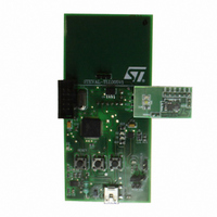
BOARD EVAL PWR FLASH STCF03/ST7
Manufacturer
STMicroelectronics
Datasheets
1.STCF03PNR.pdf
(35 pages)
2.STEVAL-TLL005V1.pdf
(4 pages)
3.STEVAL-TLL005V1.pdf
(10 pages)
Specifications of STEVAL-TLL005V1
Design Resources
STEVAL-TLL005V1 Bill of Materials
Main Purpose
Lighting, Camera Flash
Embedded
Yes, MCU, 8-Bit
Utilized Ic / Part
STCF03
Primary Attributes
Camera Flash, I2C Controlled, Flash and Torch Mode
Secondary Attributes
Li-Ion Battery, Battery Charger Circuit, GUI
Description/function
Flash Driver Evaluation Board
Core Chip
STCF03
Topology
Buck-Boost
No. Of Outputs
1
Dimming Control Type
I2C
Development Tool Type
Hardware - Eval/Demo Board
Supported Devices
STCF03 Device Type
For Use With
497-8431 - BOARD EVAL FLASH DRIVER STCF03
Lead Free Status / RoHS Status
Lead free / RoHS Compliant
For Use With/related Products
STCF03, ST7
Other names
497-8207


STCF03
7
7.1
7.2
7.2.1
7.2.2
7.2.3
Introduction
The STCF03 is a buck-boost converter, dedicated to power and control the current of a
power white LED in a camera cell phone. The device operates at a constant switching
frequency of 1.8 MHz typ. It provides an output voltage down to 2.5 V and up to 5.3 V, from
a 2.7 V to 5.5 V supply voltage. This supply range allows operation from a single cell
Lithium-Ion battery. The I²C bus is used to control the device operation and for diagnostic
purposes. The current in torch mode is adjustable from 15 mA to 200 mA. Flash mode
current is adjustable up to 800 mA, BGA version is able to deliver 600 mA at battery range
2.7 V to 3.3 V. The Aux LED current can be adjusted from 0 to 20 mA. The device uses an
external NTC resistor to sense the temperature of the white LED. These two last functions
may not be needed in all applications, and in these cases the relevant external components
can be omitted.
Buck-boost converter
The regulation of the PWM controller is done by sensing the current of the LED through
external sensing resistors (R
forward voltage of the flash LED, the device automatically can change the operation mode
between buck (step down) and boost (step up) mode.
Three cases can occur: boost region (V
cases, as the output voltage V
< V
Logic pin description
SCL, SDA pins
These are the standard clock and data pins as defined in the I²C bus specification. External
pull-up is required according to I²C bus specifications. The recommended maximum voltage
of these signals should be 3.0 V.
TRIG pin
This input pin is internally AND-ed with the TRIG_EN bit to generate the internal signal that
activates the flash operation. This gives to the user the possibility to accurately control the
flash duration using a dedicated pin, avoiding the I²C bus latencies (hard-triggering). No
internal pull-up nor pull-down is provided.
ATN pin
This output pin (open-drain, active LOW) is provided to better manage the information
transfer from the STCF03 to the microprocessor. Because of the limitations of a single
master I²C bus configuration, the microprocessor should regularly poll the STCF03 to verify
if certain operations have been completed, or to check diagnostic information. Alternatively,
the microprocessor can use the ATN pin to be advised that new data are available in the
STAT_REG, thus avoiding continuous polling. Then the information can be read in the
STAT_REG by a read operation via I²C that, besides, automatically resets the ATN pin. The
STAT_REG bits affecting the ATN pin status are mapped in
provided.
BAT
); buck - boost region (V
FL
O
Doc ID 13169 Rev 7
O
and R
= V
~ V
fLED
BAT
TR
).
O
, see application schematic). Depending on the
+ I
> V
LED
BAT
x RFL) is higher than V
): this configuration is used in most of the
Table
16. No internal pull-up is
BAT
; buck region (V
Introduction
13/35
O
Related parts for STEVAL-TLL005V1
Image
Part Number
Description
Manufacturer
Datasheet
Request
R

Part Number:
Description:
BOARD EVAL FOR ST802RT1
Manufacturer:
STMicroelectronics
Datasheet:

Part Number:
Description:
EVAL BOARD 100 BASE T
Manufacturer:
STMicroelectronics
Datasheet:

Part Number:
Description:
BOARD ELECT FISCAL CASH REGISTER
Manufacturer:
STMicroelectronics
Datasheet:
Part Number:
Description:
BOARD EVAL FOR ST802RT1A
Manufacturer:
STMicroelectronics
Datasheet:

Part Number:
Description:
2 kW/100 V RF demonstration board for 3 T MRI based on the STAC4932B
Manufacturer:
STMICROELECTRONICS [STMicroelectronics]
Datasheet:

Part Number:
Description:
BOARD EVAL FOR MEMS SENSORS
Manufacturer:
STMicroelectronics
Datasheet:
Part Number:
Description:
EVALBOARD/STEVAL-ISV014V1
Manufacturer:
STMicroelectronics

Part Number:
Description:
BOARD EVAL FOR VACUUM CLEANER
Manufacturer:
STMicroelectronics
Datasheet:

Part Number:
Description:
KIT DEV STARTER ST10F276Z5
Manufacturer:
STMicroelectronics
Datasheet:

Part Number:
Description:
BOARD LED CTLR/DVR STLED316S
Manufacturer:
STMicroelectronics
Datasheet:
Part Number:
Description:
STMicroelectronics [RIPPLE-CARRY BINARY COUNTER/DIVIDERS]
Manufacturer:
STMicroelectronics
Datasheet:
Part Number:
Description:
STMicroelectronics [LIQUID-CRYSTAL DISPLAY DRIVERS]
Manufacturer:
STMicroelectronics
Datasheet:
Part Number:
Description:
BOARD EVAL FOR MEMS SENSORS
Manufacturer:
STMicroelectronics
Datasheet: