STEVAL-IFP007V1 STMicroelectronics, STEVAL-IFP007V1 Datasheet - Page 10
STEVAL-IFP007V1
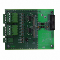
Manufacturer Part Number
STEVAL-IFP007V1
Description
BOARD EVAL BASED ON SCLT3-8
Manufacturer
STMicroelectronics
Specifications of STEVAL-IFP007V1
Main Purpose
Interface, Digital Signal Termination
Embedded
No
Utilized Ic / Part
SCLT3-8
Primary Attributes
8 Channel Optical Isolation
Secondary Attributes
SPI Interface
Processor To Be Evaluated
SCLT3
Data Bus Width
16 bit
Interface Type
SPI
Operating Supply Voltage
24 V
Lead Free Status / RoHS Status
Lead free / RoHS Compliant
Other names
497-9045


Functional description
2.5
2.5.1
2.5.2
2.5.3
2.5.4
10/33
SPI bus signal description
Chip select /CS
When the chip select signal /CS is high, the data transfer is disabled (SCK and MOSI
signals are ignored) and the data output MISO is in high impedance tri-state Z.
Driving this input low enables the communication process. At each falling edge of the /CS,
the 8 input logic states, and the 8 control bits are loaded into the SPI shift register.
The chip select /CS must toggle only when the serial clock signal SCK is in low state.
Serial clock SCK
This clock signal defines the speed and sequence of the SPI communication and is
controlled by the master unit. Its transient edges define the serial protocol operation:
●
●
The SCLT internal circuitry secures the SPI operation in mode C
the chip select /CS falls low, the first edge of the clock SCK to be active is always the rising
edge.
Figure 8.
Serial data input MOSI
This input signal MOSI is used to shift external data bits into the SCLT register from the
most significant (MSB) bit to the least significant one (LSB). The data bits are captured by
the SCLT on the rising edge of the serial clock signal SCK.
Like the clock SCK, and the chip select /CS, the MOSI input circuit is filtered as shown in
Figure
of the SPI circuit.
Serial data output MISO
This output signal is used to transfer data out of the SCLT slave circuit from the most
significant bit (MSB) to the least significant bit (LSB). The first data bit is written out when
the chip select /CS goes low. Then the other data bits are written out on the falling edge of
the clock signal SCK.
The output MISO goes to high impedance tri-state shown on
goes in high state.
The falling edge generates the shift of the data in the register and the last bit writing on
the output MISO.
The rising edge generates the capture of the data on the input MOSI.
8, in order to match maximum speed operation and improve the EFT burst immunity
Functional diagram of the SPI logic inputs SCK, MOSI, /CS
SCK
Doc ID 15191 Rev 3
ESD HBM
2kΩ
250kΩ
V
DD
2pF
SCLT3-8
Table 5
POL
= 0, C
when the /CS signal
PHA
SCLT3-8BT8
= 0. When
Related parts for STEVAL-IFP007V1
Image
Part Number
Description
Manufacturer
Datasheet
Request
R

Part Number:
Description:
BOARD EVAL SPZB260 MOD FOR STR9
Manufacturer:
STMicroelectronics
Datasheet:

Part Number:
Description:
BOARD EVAL EXTENSION SN250
Manufacturer:
STMicroelectronics
Datasheet:

Part Number:
Description:
BOARD EVAL AB-54003L-512
Manufacturer:
STMicroelectronics
Datasheet:

Part Number:
Description:
BOARD REF DESIGN RF DMOS PWR AMP
Manufacturer:
STMicroelectronics
Datasheet:

Part Number:
Description:
BOARD EVAL PWR AMP AB-84008L-470
Manufacturer:
STMicroelectronics
Datasheet:

Part Number:
Description:
BOARD EVAL FOR STM32F103XX
Manufacturer:
STMicroelectronics
Datasheet:

Part Number:
Description:
BOARD EVAL AB-54003L-512
Manufacturer:
STMicroelectronics
Datasheet:

Part Number:
Description:
BOARD SMART PLUG STM32 SPZB260PR
Manufacturer:
STMicroelectronics
Datasheet:

Part Number:
Description:
BOARD DEMO BLUETOOTH SPBT2532C2
Manufacturer:
STMicroelectronics
Datasheet:
Part Number:
Description:
ZIGBEE USB DONGLE EVAL KIT
Manufacturer:
STMicroelectronics
Datasheet:
Part Number:
Description:
STMicroelectronics [RIPPLE-CARRY BINARY COUNTER/DIVIDERS]
Manufacturer:
STMicroelectronics
Datasheet:
Part Number:
Description:
STMicroelectronics [LIQUID-CRYSTAL DISPLAY DRIVERS]
Manufacturer:
STMicroelectronics
Datasheet:

Part Number:
Description:
BOARD EVAL FOR MEMS SENSORS
Manufacturer:
STMicroelectronics
Datasheet: