SI5338-EVB Silicon Laboratories Inc, SI5338-EVB Datasheet - Page 32
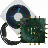
SI5338-EVB
Manufacturer Part Number
SI5338-EVB
Description
BOARD EVALUATION SI5338
Manufacturer
Silicon Laboratories Inc
Datasheet
1.SI5338B-A-GM.pdf
(42 pages)
Specifications of SI5338-EVB
Main Purpose
Timing, Clock Generator
Embedded
No
Utilized Ic / Part
Si5338
Primary Attributes
160 kHz to 700 MHz in LVPECL/LVDS,
Secondary Attributes
USB Based GUI to Program, I2C/SMBus Compatible Interface, 1.8, 2.5, or 3.3 V
For Use With/related Products
Si5330/34/38 Family
Lead Free Status / RoHS Status
Lead free / RoHS Compliant
Lead Free Status / RoHS Status
Lead free / RoHS Compliant, Lead free / RoHS Compliant
Other names
336-1556


Si5338
32
Pin #
3
4
Pin Name
IN3
IN4
I/O
I
I
Table 15. Si5338 Pin Descriptions (Continued)
Signal Type
Multi
Multi
This pin can have one of the following functions depending on the
part number:
CLKIN (for Si5338A/B/C and Si5338N/P/Q devices only)
Provides a high-impedance clock input for single ended clock
signals. This input should be dc-coupled as shown in “3.2. Input
Stage”, Figure 3.
If this pin is not used, it should be connected to ground.
PINC (for Si5338D/E/F devices only)
Used as the phase increment pin. See "3.10.2. Output Phase
Increment/Decrement" on page 25 for more details. Minimum
pulse width of 100 ns is required for proper operation. If this pin is
not used, it should be connected to ground.
FINC (for Si5338G/H/J devices only)
Used as the frequency increment pin. See "3.10.1. Frequency
Increment/Decrement" on page 25 for more details. Minimum
pulse width of 100 ns is required for proper operation. If this pin is
not used, it should be connected to ground.
OEB (for Si5338K/L/M devices only)
Used as an output enable pin. 0 = All outputs enabled; 1 = All
outputs disabled. By default, outputs are tri-stated when disabled.
This pin can have one of the following functions depending on the
part number
I
This is the LSB of the Si5338 I
70h (111 0000), 1 = I
FDBK (for Si5338N/P/Q devices only)
Provides a high-impedance feedback input for single-ended clock
signals. This input should be dc-coupled as shown in “3.2. Input
Stage”, Figure 3. If this pin is not used, it should be connected to
ground.
PDEC (for Si5338D/E/F) devices only)
Used as the phase decrement pin. See “3.10.2. Output Phase
Increment/Decrement” for more details. Minimum pulse width of
100 ns is required for proper operation. If this pin is not used, it
should be connected to ground.
FDEC (for Si5338G/H/J devices only)
Used as the frequency decrement pin. See “3.10.1. Frequency
Increment/Decrement” for more details. Minimum pulse width of
100 ns is required for proper operation. If this pin is not used, it
should be connected to ground.
2
C_LSB (for Si5338A/B/C and Si5338K/L/M devices only)
Rev. 1.0
2
C address 71h (111 0001).
Description
2
C address. 0 = I
2
C address
Related parts for SI5338-EVB
Image
Part Number
Description
Manufacturer
Datasheet
Request
R

Part Number:
Description:
KIT PROG FIELD SI5338/4/0
Manufacturer:
Silicon Laboratories Inc
Datasheet:

Part Number:
Description:
Programmers & Debuggers Si5338/4/0 field programming kit
Manufacturer:
Silicon Laboratories Inc
Datasheet:
Part Number:
Description:
SMD/C°/SINGLE-ENDED OUTPUT SILICON OSCILLATOR
Manufacturer:
Silicon Laboratories Inc
Part Number:
Description:
Manufacturer:
Silicon Laboratories Inc
Datasheet:
Part Number:
Description:
N/A N/A/SI4010 AES KEYFOB DEMO WITH LCD RX
Manufacturer:
Silicon Laboratories Inc
Datasheet:
Part Number:
Description:
N/A N/A/SI4010 SIMPLIFIED KEY FOB DEMO WITH LED RX
Manufacturer:
Silicon Laboratories Inc
Datasheet:
Part Number:
Description:
N/A/-40 TO 85 OC/EZLINK MODULE; F930/4432 HIGH BAND (REV E/B1)
Manufacturer:
Silicon Laboratories Inc
Part Number:
Description:
EZLink Module; F930/4432 Low Band (rev e/B1)
Manufacturer:
Silicon Laboratories Inc
Part Number:
Description:
I°/4460 10 DBM RADIO TEST CARD 434 MHZ
Manufacturer:
Silicon Laboratories Inc
Part Number:
Description:
I°/4461 14 DBM RADIO TEST CARD 868 MHZ
Manufacturer:
Silicon Laboratories Inc
Part Number:
Description:
I°/4463 20 DBM RFSWITCH RADIO TEST CARD 460 MHZ
Manufacturer:
Silicon Laboratories Inc
Part Number:
Description:
I°/4463 20 DBM RADIO TEST CARD 868 MHZ
Manufacturer:
Silicon Laboratories Inc
Part Number:
Description:
I°/4463 27 DBM RADIO TEST CARD 868 MHZ
Manufacturer:
Silicon Laboratories Inc
Part Number:
Description:
I°/4463 SKYWORKS 30 DBM RADIO TEST CARD 915 MHZ
Manufacturer:
Silicon Laboratories Inc