DTMFDECODER-RD Silicon Laboratories Inc, DTMFDECODER-RD Datasheet - Page 103
DTMFDECODER-RD
Manufacturer Part Number
DTMFDECODER-RD
Description
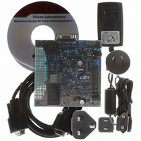
KIT REF DESIGN DTMF DECODER
Manufacturer
Silicon Laboratories Inc
Specifications of DTMFDECODER-RD
Mfg Application Notes
DTMF Decoder Ref Design AppNote
Main Purpose
Telecom, DTMF Decoder
Embedded
No
Utilized Ic / Part
C8051F300
Primary Attributes
8kHz Sampling Rate ADC
Secondary Attributes
16 Goertzel Filters
Processor To Be Evaluated
C8051F300
Interface Type
RS-232
Lead Free Status / RoHS Status
Contains lead / RoHS non-compliant
Lead Free Status / RoHS Status
Lead free / RoHS Compliant, Contains lead / RoHS non-compliant
Other names
336-1283


12. Port Input/Output
Digital and analog resources are available through a byte-wide digital I/O Port, Port0. Each of the Port pins
can be defined as general-purpose I/O (GPIO), analog input, or assigned to one of the internal digital
resources as shown in Figure 12.3. The designer has complete control over which functions are assigned,
limited only by the number of physical I/O pins. This resource assignment flexibility is achieved through the
use of a Priority Crossbar Decoder. Note that the state of a Port I/O pin can always be read in the corre-
sponding Port latch, regardless of the Crossbar settings.
The Crossbar assigns the selected internal digital resources to the I/O pins based on the Priority Decoder
(Figure 12.3 and Figure 12.4). The registers XBR0, XBR1, and XBR2, defined in SFR Definition 12.1, SFR
Definition 12.2, and SFR Definition 12.3 are used to select internal digital functions.
All Port I/Os are 5 V tolerant (refer to Figure 12.2 for the Port cell circuit). The Port I/O cells are configured
as either push-pull or open-drain in the Port0 Output Mode register (P0MDOUT). Complete Electrical
Specifications for Port I/O are given in Table 12.1 on page 110.
Highest
Priority
Lowest
Priority
/WEAK-PULLUP
PUSH-PULL
/PORT-OUTENABLE
PORT-OUTPUT
ANALOG INPUT
PORT-INPUT
Figure 12.1. Port I/O Functional Block Diagram
SYSCLK
Outputs
SMBus
T0, T1
UART
PCA
CP0
Figure 12.2. Port I/O Cell Block Diagram
Port Latch
2
2
2
4
2
P0
Analog Select
(P0.0-P0.7)
8
Rev. 2.9
XBR2 Registers
XBR0, XBR1,
Crossbar
Decoder
Priority
Digital
C8051F300/1/2/3/4/5
8
P0MDIN Registers
GND
VDD
P0MDOUT,
Cells
P0
I/O
VDD
(WEAK)
P0.0
P0.7
PORT
PAD
103
Related parts for DTMFDECODER-RD
Image
Part Number
Description
Manufacturer
Datasheet
Request
R

Part Number:
Description:
SMD/C°/SINGLE-ENDED OUTPUT SILICON OSCILLATOR
Manufacturer:
Silicon Laboratories Inc
Part Number:
Description:
Manufacturer:
Silicon Laboratories Inc
Datasheet:
Part Number:
Description:
N/A N/A/SI4010 AES KEYFOB DEMO WITH LCD RX
Manufacturer:
Silicon Laboratories Inc
Datasheet:
Part Number:
Description:
N/A N/A/SI4010 SIMPLIFIED KEY FOB DEMO WITH LED RX
Manufacturer:
Silicon Laboratories Inc
Datasheet:
Part Number:
Description:
N/A/-40 TO 85 OC/EZLINK MODULE; F930/4432 HIGH BAND (REV E/B1)
Manufacturer:
Silicon Laboratories Inc
Part Number:
Description:
EZLink Module; F930/4432 Low Band (rev e/B1)
Manufacturer:
Silicon Laboratories Inc
Part Number:
Description:
I°/4460 10 DBM RADIO TEST CARD 434 MHZ
Manufacturer:
Silicon Laboratories Inc
Part Number:
Description:
I°/4461 14 DBM RADIO TEST CARD 868 MHZ
Manufacturer:
Silicon Laboratories Inc
Part Number:
Description:
I°/4463 20 DBM RFSWITCH RADIO TEST CARD 460 MHZ
Manufacturer:
Silicon Laboratories Inc
Part Number:
Description:
I°/4463 20 DBM RADIO TEST CARD 868 MHZ
Manufacturer:
Silicon Laboratories Inc
Part Number:
Description:
I°/4463 27 DBM RADIO TEST CARD 868 MHZ
Manufacturer:
Silicon Laboratories Inc
Part Number:
Description:
I°/4463 SKYWORKS 30 DBM RADIO TEST CARD 915 MHZ
Manufacturer:
Silicon Laboratories Inc
Part Number:
Description:
N/A N/A/-40 TO 85 OC/4463 RFMD 30 DBM RADIO TEST CARD 915 MHZ
Manufacturer:
Silicon Laboratories Inc
Part Number:
Description:
I°/4463 20 DBM RADIO TEST CARD 169 MHZ
Manufacturer:
Silicon Laboratories Inc