EVAL-AD9832EBZ Analog Devices Inc, EVAL-AD9832EBZ Datasheet - Page 8
EVAL-AD9832EBZ
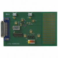
Manufacturer Part Number
EVAL-AD9832EBZ
Description
BOARD EVAL FOR AD9832
Manufacturer
Analog Devices Inc
Specifications of EVAL-AD9832EBZ
Main Purpose
Timing, Direct Digital Synthesis (DDS)
Embedded
No
Utilized Ic / Part
AD9832
Primary Attributes
10-Bit DAC, 32-Bit Tuning Word Width
Secondary Attributes
25MHz, Graphical User Interface, 2.97 V ~ 5.5 V
Lead Free Status / RoHS Status
Lead free / RoHS Compliant
Other names
EVAL-AD9832EB
EVAL-AD9832EB
EVAL-AD9832EB


AD9832
TERMINOLOGY
Integral Nonlinearity
This is the maximum deviation of any code from a straight line
passing through the endpoints of the transfer function. The end-
points of the transfer function are zero scale, a point 0.5 LSB be-
low the first code transition (000 . . . 00 to 000 . . . 01) and full
scale, a point 0.5 LSB above the last code transition (111 . . . 10
to 111 . . . 11). The error is expressed in LSBs.
Differential Nonlinearity
This is the difference between the measured and ideal 1 LSB
change between two adjacent codes in the DAC.
Signal to (Noise + Distortion)
Signal to (Noise + Distortion) is measured signal to noise at the
output of the DAC. The signal is the rms magnitude of the
fundamental. Noise is the rms sum of all the nonfundamental
signals up to half the sampling frequency (f
ing the dc component. Signal to (Noise + Distortion) is depen-
dent on the number of quantization levels used in the digitization
process; the more levels, the smaller the quantization noise. The
theoretical Signal to (Noise + Distortion) ratio for a sine wave
input is given by
where N is the number of bits. Thus, for an ideal 10-bit con-
verter, Signal to (Noise + Distortion) = 61.96 dB.
Total Harmonic Distortion
Total Harmonic Distortion (THD) is the ratio of the rms
sum of harmonics to the rms value of the fundamental. For
the AD9832, THD is defined as:
where V
V
sixth harmonic.
Output Compliance
The output compliance refers to the maximum voltage that can
be generated at the output of the DAC to meet the specifica-
tions. When voltages greater than those specified for the output
compliance are generated, the AD9832 may not meet the speci-
fications listed in the data sheet.
Spurious Free Dynamic Range
Along with the frequency of interest, harmonics of the fundamental
frequency and images of the MCLK frequency are present at the
output of a DDS device. The spurious free dynamic range (SFDR)
refers to the largest spur or harmonic present in the band of
interest. The wide band SFDR gives the magnitude of the larg-
est harmonic or spur relative to the magnitude of the fundamental
frequency in the bandwidth 2 MHz about the fundamental fre-
quency. The narrow band SFDR gives the attenuation of the
largest spur or harmonic in a bandwidth of 50 kHz about the
fundamental frequency.
Clock Feedthrough
There will be feedthrough from the MCLK input to the analog
output. Clock feedthrough refers to the magnitude of the MCLK
signal relative to the fundamental frequency in the AD9832’s out-
put spectrum.
4
, V
5
and V
Signal to (Noise + Distortion) = (6.02N + 1.76) dB
THD
1
is the rms amplitude of the fundamental and V
6
are the rms amplitudes of the second through the
20 log
V
2
2
V
3
2
V
V
1
4
2
MCLK
V
5
2
/2) but exclud-
V
6
2
2
, V
3
,
–8–
A3
0
0
0
0
0
0
0
0
1
1
1
1
1
1
1
1
Register
FREQ0 REG
FREQ1 REG
PHASE0 REG 12 Bits
PHASE1 REG 12 Bits
PHASE2 REG 12 Bits
PHASE3 REG 12 Bits
8
4
H
M
- 8
M
S
B
A2
0
0
0
0
1
1
1
1
0
0
0
0
1
1
1
1
S
B
t i
B
6 1
s
W
s
(
T
M
Table II. Addressing the Registers
o
Table III. 32-Bit Frequency Word
Table IV. 12-Bit Frequency Word
h
r
S
e
d
Size
32 Bits
32 Bits
B
8
A1
0
0
1
1
0
0
1
1
0
0
1
1
0
0
1
1
Table I. Control Registers
4
L
s
L
o
M
a
M
S
d
B
S
e
d
B
s
=
s
f o
A0
0
1
0
1
0
1
0
1
0
1
0
1
0
1
0
1
Description
Frequency Register 0. This de-
fines the output frequency, when
FSELECT = 0, as a fraction of
the MCLK frequency.
Frequency Register 1. This de-
fines the output frequency, when
FSELECT = 1, as a fraction of
the MCLK frequency.
Phase Offset Register 0. When
PSEL0 = PSEL1 = 0, the contents
of this register are added to the
output of the phase accumulator.
Phase Offset Register 1. When
PSEL0 = 1 and PSEL1 = 0, the
contents of this register are added to
the output of the phase accumulator.
Phase Offset Register 2. When
PSEL0 = 0 and PSEL1 = 1, the con-
tents of this register are added to
the output of the phase accumulator.
Phase Offset Register 3. When
PSEL0 = PSEL1 = 1, the contents
of this register are added to the
output of the phase accumulator.
) 0
h t
e
8
H
Destination Register
FREQ0 REG 8 L LSBs
FREQ0 REG 8 H LSBs
FREQ0 REG 8 L MSBs
FREQ0 REG 8 H MSBs
FREQ1 REG 8 L LSBs
FREQ1 REG 8 H LSBs
FREQ1 REG 8 L MSBs
FREQ1 REG 8 H MSBs
PHASE0 REG 8 LSBs
PHASE0 REG 8 MSBs
PHASE1 REG 8 LSBs
PHASE1 REG 8 MSBs
PHASE2 REG 8 LSBs
PHASE2 REG 8 MSBs
PHASE3 REG 8 LSBs
PHASE3 REG 8 MSBs
L
S
B
6 1
s
L
8
S
L
B
8
S
s
B
L
s
L
S
REV. A
B
s
Related parts for EVAL-AD9832EBZ
Image
Part Number
Description
Manufacturer
Datasheet
Request
R


Part Number:
Description:
BOARD EVAL FOR SI270X-A
Manufacturer:
Silicon Laboratories Inc
Datasheet:

Part Number:
Description:
BUCK CONV REF DESIGN KIT IP1201
Manufacturer:
International Rectifier
Datasheet:
Part Number:
Description:
BOARD DEMO SYNC DUAL BUCK CNVTER
Manufacturer:
International Rectifier
Datasheet:
Part Number:
Description:
BOARD DEMO SYNC BUCK CONVETER
Manufacturer:
International Rectifier
Datasheet:

Part Number:
Description:
EVALBOARD/EB Omnidirectional microphone - Analog
Manufacturer:
Analog Devices
Datasheet:
Part Number:
Description:
EVALBOARD/EB Omnidirectional microphone - Analog
Manufacturer:
Analog Devices
Datasheet:


Part Number:
Description:
BOARD EVAL LED DRIVER LT3756
Manufacturer:
Linear Technology
Datasheet:

Part Number:
Description:
BOARD EVAL FOR AD7741/7742
Manufacturer:
Analog Devices Inc
Datasheet:

Part Number:
Description:
±1.7g Dual-Axis IMEMS Accelerometer Evaluation Board
Manufacturer:
Analog Devices Inc
Datasheet:

Part Number:
Description:
IC MULTIPLIER ANALOG 8-SOIC T/R
Manufacturer:
Analog Devices Inc
Datasheet:

Part Number:
Description:
IC ANALOG MULTIPLIER 8-DIP
Manufacturer:
Analog Devices Inc
Datasheet:
Part Number:
Description:
IC ANALOG MULTIPLIER 8-SOIC
Manufacturer:
Analog Devices Inc
Datasheet:
Part Number:
Description:
IC ANALOG MULTIPLIER 8-DIP
Manufacturer:
Analog Devices Inc
Datasheet: