EVAL-AD7877EBZ Analog Devices Inc, EVAL-AD7877EBZ Datasheet - Page 30
EVAL-AD7877EBZ
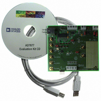
Manufacturer Part Number
EVAL-AD7877EBZ
Description
BOARD EVALUATION FOR AD7877
Manufacturer
Analog Devices Inc
Datasheets
1.AD7877ACBZ-REEL7.pdf
(44 pages)
2.EVAL-AD7877EBZ.pdf
(16 pages)
3.EVAL-AD7877EBZ.pdf
(44 pages)
Specifications of EVAL-AD7877EBZ
Main Purpose
Interface, Touch Screen Controller
Embedded
No
Utilized Ic / Part
AD7877
Primary Attributes
4-Wire Resistive Touch Screen Controller, SPI Interface, On-Chip: Temp Sensor, Voltage Reference, 8-Bit DAC
Secondary Attributes
USB GUI, LCD Noise Reduction Feature, 2.7 ~ 5.25 V, Wake Up on Touch Feature
Lead Free Status / RoHS Status
Lead free / RoHS Compliant


AD7877
GENERAL-PURPOSE I/O PINS
The AD7877 has one dedicated general-purpose logic input/
output pin (GPIO4), and any or all of the three auxiliary analog
inputs can also be reconfigured as GPIOs. Associated with the
GPIOs are two 8-bit control registers and one 8-bit data register
that are accessed using the extended write mode.
As described in the Reading Data section, GPIO registers are
written to using the extended writing mode. The first four bits
of the data-word must be 1111b to access the extended writing
map, and the next four bits are the GPIO register address. This
leaves 8 bits for the GPIO register data, because all GPIO
registers are 8 bits.
The GPIO control registers are located at the 0000b and 0001b
extended writing map addresses, and the GPIO data register is
at Address 0010b. GPIO registers are read in the same way as
other registers, by writing a 5-bit address to Control Register 1.
The GPIO registers are located at Read Addresses 11011b to
Read Address 11101b.
GPIO CONFIGURATION
Each GPIO pin is configured by four bits in one of the GPIO
control registers and has a data bit in the GPIO data register.
The GPIO configuration bits are described in the following
sections and in Table 12. Also see the Detailed Register
Descriptions section.
Enable (EN)
These bits enable or disable the GPIO pins. When EN = 0, the
corresponding GPIO pin is configured as the alternate function
(AUX input). The other GPIO configuration bits have no effect,
if the particular GPIO is not enabled. When EN = 1, the pin is
configured as a GPIO pin. GPIO4, which does not have an
alternate function, does not have an EN bit; it is always enabled.
Direction—DIR
These bits set the direction of the GPIO pins. When DIR = 0,
the pin is an output. Setting or clearing the relevant bit in the
GPIO data register outputs a value on the corresponding GPIO
pin. The output value depends on the POL bit.
When DIR = 1, the pin is an input. An input value on the
relevant GPIO pin sets or clears the corresponding bit in the
GPIO data register, depending on the POL bit. A GPIO data
register bit is read-only when DIR = 1 for that GPIO.
Polarity (POL)
When POL = 0, the GPIO pin is active low. When POL = 1, the
GPIO pin is active high. How this bit affects the GPIO opera-
tion also depends on the DIR bit.
If POL = 1 and DIR = 1, a 1 at the input pin sets the corre-
sponding GPIO data register bit to 1. A 0 at the input pin clears
the corresponding GPIO data bit to 0.
Rev. C | Page 30 of 44
If POL = 1 and DIR = 0, a 1 in the GPIO data register bit puts a
1 on the corresponding GPIO output pin. A 0 in the GPIO data
register bit puts a 0 on the GPIO output pin.
If POL = 0 and DIR = 1, a 1 at the input pin sets the corre-
sponding GPIO data bit to 0. A 0 at the input pin clears the
corresponding GPIO data bit to 1.
If POL = 0 and DIR = 0, a 1 in the GPIO data register bit puts a
0 on the corresponding GPIO output pin. A 0 in the GPIO data
register bit puts a 1 on the GPIO output pin.
ALERT Enable (ALEN)
GPIOs can operate as interrupt sources to trigger the ALERT
output. This is controlled by the ALERT enable (ALEN) bits in
the GPIO configuration registers. When ALEN = 1, the corre-
sponding GPIO can trigger an ALERT . When ALEN = 0, the
corresponding GPIO cannot cause the ALERT output to assert.
ALERT is asserted low if any GPIO data register bit is set when
the GPIO is configured as an input. The GPIO data bit is set if a
1 appears on the GPIO input pin when POL = 1, or if a 0
appears on the GPIO input pin when POL = 0. ALERT is
triggered only when the GPIO is configured as an input, that is,
when DIR = 1. ALERT can never be triggered by a GPIO that is
configured as an output, that is, DIR = 0.
ALERT Output
The ALERT pin is an alarm or interrupt output that goes low if
any one of a number of interrupt sources is asserted. The results
of high and low limit comparisons on the AUX1, BAT1, BAT2,
and TEMP1 channels are interrupt sources. An out-of-limit
comparison sets a status bit in the alert status/mask register
(Address 00011b).There are separate status bits for both the
high and low limits on each channel to indicate which limit was
exceeded. The interrupt sources can be masked out by clearing
the corresponding enable bit in this register. There is one enable
bit per channel.
ALERT is also asserted if an input on a GPIO pin sets a bit in
the GPIO data register, as explained in the ALERT Enable
(ALEN) section. GPIO interrupts can be disabled by clearing
the corresponding ALEN bit in the GPIO control registers.
The interrupt source can be identified by reading the GPIO data
register and the alert status/enable register. ALERT remains
asserted until the source of the interrupt has been masked out
or removed.
Related parts for EVAL-AD7877EBZ
Image
Part Number
Description
Manufacturer
Datasheet
Request
R


Part Number:
Description:
BOARD EVAL FOR SI270X-A
Manufacturer:
Silicon Laboratories Inc
Datasheet:

Part Number:
Description:
BUCK CONV REF DESIGN KIT IP1201
Manufacturer:
International Rectifier
Datasheet:
Part Number:
Description:
BOARD DEMO SYNC DUAL BUCK CNVTER
Manufacturer:
International Rectifier
Datasheet:
Part Number:
Description:
BOARD DEMO SYNC BUCK CONVETER
Manufacturer:
International Rectifier
Datasheet:

Part Number:
Description:
EVALBOARD/EB Omnidirectional microphone - Analog
Manufacturer:
Analog Devices
Datasheet:
Part Number:
Description:
EVALBOARD/EB Omnidirectional microphone - Analog
Manufacturer:
Analog Devices
Datasheet:


Part Number:
Description:
BOARD EVAL LED DRIVER LT3756
Manufacturer:
Linear Technology
Datasheet:

Part Number:
Description:
BOARD EVAL FOR AD7741/7742
Manufacturer:
Analog Devices Inc
Datasheet:

Part Number:
Description:
±1.7g Dual-Axis IMEMS Accelerometer Evaluation Board
Manufacturer:
Analog Devices Inc
Datasheet:

Part Number:
Description:
IC MULTIPLIER ANALOG 8-SOIC T/R
Manufacturer:
Analog Devices Inc
Datasheet:

Part Number:
Description:
IC ANALOG MULTIPLIER 8-DIP
Manufacturer:
Analog Devices Inc
Datasheet:
Part Number:
Description:
IC ANALOG MULTIPLIER 8-SOIC
Manufacturer:
Analog Devices Inc
Datasheet:
Part Number:
Description:
IC ANALOG MULTIPLIER 8-DIP
Manufacturer:
Analog Devices Inc
Datasheet: